
Processing Example
Si Deep RIE
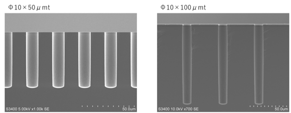
Fig. 1. Si Deep RIE example: 10 µm-diameter Si holes etched to depths of 50 µm and 100 µm.
TSV Copper Filling
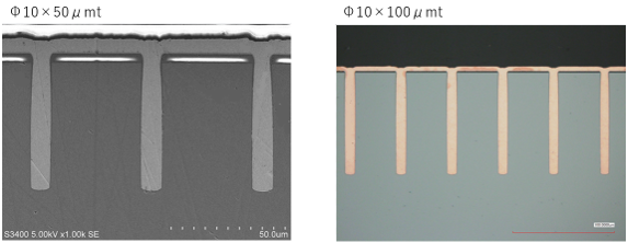
Fig. 2. TSV copper filling example: Cu-filled vias with a diameter of 10 µm and depths of 50 µm and 100 µm.
Photolithography
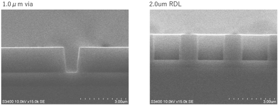
Fig. 3. Fine photolithography examples: 1.0 µm via and 2.0 µm RDL patterns.
Insulating Film Dry Etching
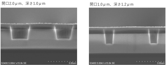
Fig. 4. Insulating film dry etching examples with micron-scale openings and depths.
Bump
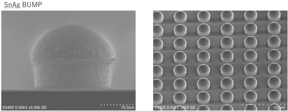
Fig. 5. SnAg solder bump formation example: cross-sectional and bump-array SEM images.
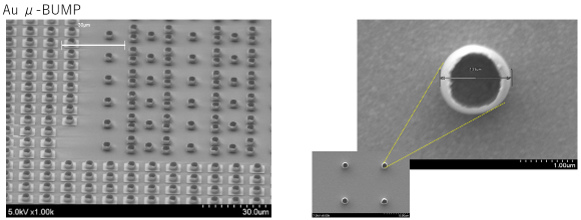
Fig. 6. Au micro-bump formation example: bump-array and magnified SEM images.