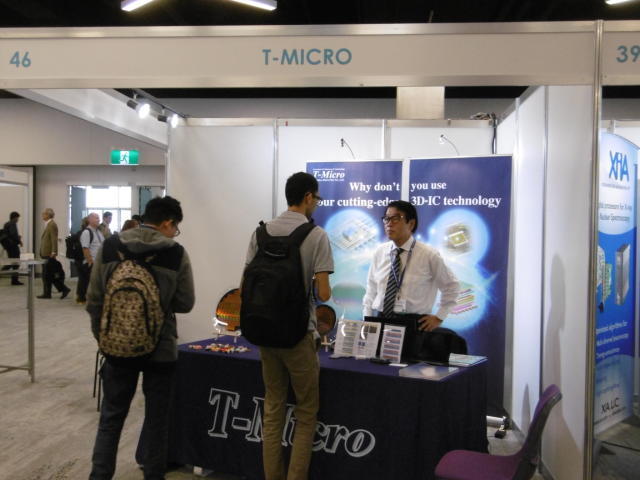

2025 CEA-Leti Innovation Days / LID World Summit
Jun. 17-19 @Grenoble, France
Dear Sir/Madam,
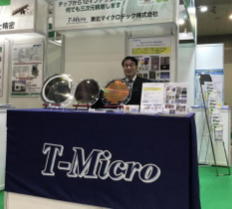
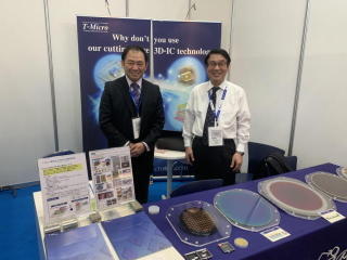
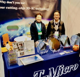
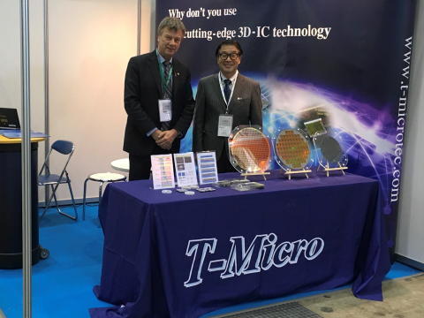
Thank you very much to everyone who visited our booth at the LID World Summit.
If you have any questions about our technology or business model, please feel free to contact me.
[info.tm@t-microtec.com]
We would also like to express our sincere gratitude to the Leti staf for their kind support.
We look forward to seeing you again next year.
Best Regards,
Makoto Motoyoshi (CEO)