
3D-stacked LSI is the next generation device which is expected to reduce power consumption down to half. From the view of clean environment, establishment of stable, secure and cost-effective technology of 3D stacked LSI is these days craved for. In anticipation of substitution for the current 2D LSI and promotion of the 3D-stacked LSI in a variety of market segments, further research and development are essential.
Tohoku-MicroTec Co., Ltd. (Tohoku-MicroTec), established at Sendai, Japan in April, 2010, is the unique and leading 3D-Stacked LSI process-oriented company, utilizing the next generation process & manufacturing technology, originated in Tohoku university, of fine-pitch Through-Silicon-VIA (TSV), Microbump, Thinning, Bonding and Alignment.
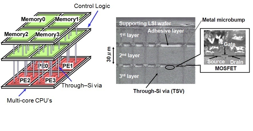
In wide and tight collaboration with New Industry Creation Hatchery Center of Tohoku University, we research and develop Bio-Electronics products for Neuroscience, provide 3D-Stacked LSI prototype manufacturing services at a drastic cost-effective way, and counsel on the development related to 3D-Stacked LSI process.