
Tohoku-MicroTec (T-Micro) provides worldwide clients (Company research div., University, Research Lab, etc) with Prototype-friendly 3D-IC foundry service.
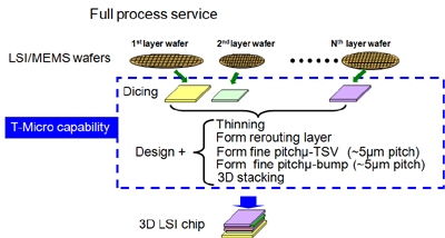
3D-IC Foundry service summary:
(Service Process)
Any or all 3D-IC process such as TSV, RDL, Bump, Thinning and Bonding.
(Service type)
Full process or Partial prcoess service
We can handle only one wafer processing or only one die processing for an initial research project.
(Stacking technology)
Wafer to Wafer (WtW)
Chip to Wafer (CtW)
Chip to Chip (CtC)
(Wafer size)
12", 8", 6", and 2" wafer
(TSV technology)
VIA-Last (Main) / VIA-First / VIA-Middle
Cu, Poly-Si (Please ask us of W !!)
Aspect ratio 1:10 (max) (Please ask us higher than 1:10 !!)
Optical TSV is available.
(Bump technology)
Various solders, Cu pillar with cap, Au, Au/In, etc (please ask us !)
(Bonding technology)
Melt, Solid Diffusion, etc (Please ask us of Direct/Fusion/Hybrid !!)
(Rerouting: RDL)
1-2 layers w/o CMP / Up to 4 layers with CMP
(Unique service)
Multi-chip bonding by Self-Assembly technology
Ultra micro-bump: Au cone/cylinder bump (>2.5um size / >5um pitch)
More info: info@t-microtec.com
Inquiry: hasegawa@t-microtec.com

English Site Menu
Company
Technology
Foundry service
Service case study