
Micro Au cone bump
We developed and released micro-sized and fine-pitch Au cone bump technology. This technology was originally developed for "Pixel detector chip" used at Electron accelerator in High Energy Laboratories. This technology contributes to great performance improvement in high-end sensor chip field such as Compound sensor, X-ray sensor, IR sensor, etc.
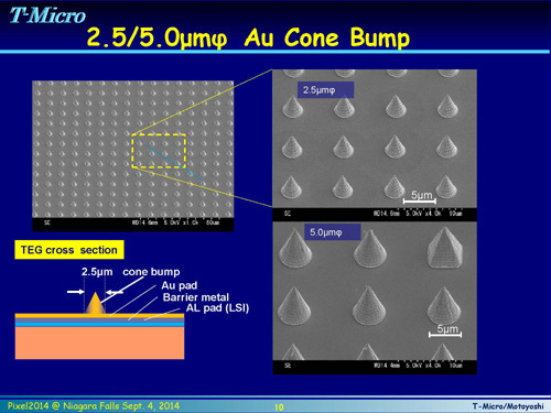
Technology definition: Au cone bump
Bump material: Au
Bump size: 2.5 x 2.5 um
Bump pitch: 5 um (min)
Advantages:
- High and flexible scalability
- Large bonding margin
- Low temperature process
Application: High-end sensor chips (Compound, X-ray, IR, SOI, etc)
Check more details from the below:
Please click (right-click for download)
- Slides: "3D Integration Technology for Pixel Detector and Image Sensor using 3-um Au Cone Bump Junctions" (Pixel2014, Sep 2014)
- Paper: "Stacked SOI Pixel Detector using Versatile Fine Pitch Micro-Bump Technology"

English Site Menu
Company
Technology
Foundry service
Service case study