
Custom Bilateral Multichannel Si Brain Probe Mfg service
We designs and manufactures Bilateral (double-sided) Multichannel Si Brain Probe, developed by use of T-MicroTec's proprietary 3DIC and MEMS process technology, for Brain Signal Recording / Stimulation. The Bilateral Multichannel Si Brain probe, named Neuronode100 series, integrates electrode sites on both Front and Back side for more effective signal recording and stimulation.
Specification :
Probe shaft material : Silicon (Si)
Electrode site material : Ir (Pt or Au optional)
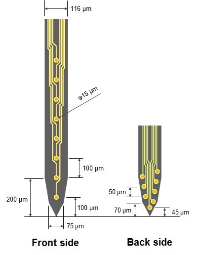
Site diameter : 10, 15, 30 um or Custom
Probe thickness : 50 um or thicker
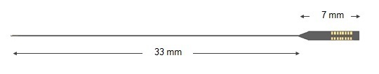
Probe length : 5, 10, 20, 33 mm or Custom
Probe width : 200 um (tapering)
Site number : Front 16 ch / Back 16 ch (Total 32 ch) or Custom
Site spacing : 50, 100, 200 um or Custom
Shank number : 1, 4 or Custom
Package : PCB / Implantable (Major system vendors compatible) or Custom
Custom Probe overview (example of 33 mm long) :
- Probe length: 5, 10, 20, 33 mm or Custom
- TSV (Through Silicon Via) and Micro-Bump connection by advanced 3D IC and MEMS process technology.
- Precise alignment between front Si substrate and back Si substrate.
- Micro-fabricated Si substrate with Ir electrode sites.
- Short width for localized measurement and minimization of tissue damage.
- Thin thickness ( less than 50 um) by unique Wafer thinning technology.
Electrode site design (exmaple of 16 ch) :
Note: Customizable of every probe parameter: dimension, length, thickness, electrode site location, shape and number, shank number, etc.
Bonding pad layout :
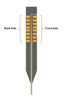
- Bonding pad layout on one side for general probe package.
Probe Package :
Acute package example :
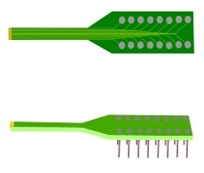
- Both Acute (PCB) and Chronic (Implantable) are available. All packages are compatible with major vendors' recording / stimulation system.
Availability :
Sample available for evaluation purpose.
Customization implemented so far : 2 cases
Download : Neuronode100 catalog
More info: info@t-microtec.com
Product example : Neuronode100 - 4 shank
Neuronode100 is the bilateral (double-sided) Si microelectrode, developed by use of T-microtec’s proprietary 3D-Stacking LSI process technology, for Brain Signal Processing Systems.Neuronode100
As shown in Fig1: Structure of Neuronode100, it integrates multichannel probe-points on both a top side and a reverse side of every probe in order to more spatially acquire electroencephalographic signals than the conventional microelectrode products.
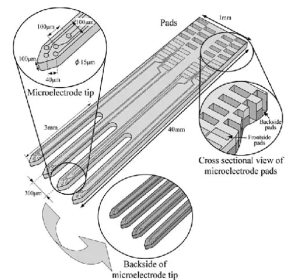
Fig1:Structure of Neuronode100
The Neuronode100’s probe-points on both sides are connected to output pads, which are connected to a processing system, through Si via. The Nueronode100 has 4 probes at a pitch of 300 μm. Each probe integrates 4 probe-points respectively on both sides. The Neuronode100 is 40 mm long, for reaching a deeper part of basal ganglia, with 100 μm wide and 100 μm thick. The probe-point is made of gold with equal length pattern Diameter of the probe-point is 15μm and the distance between the probe-points is 40 μm in center to center.
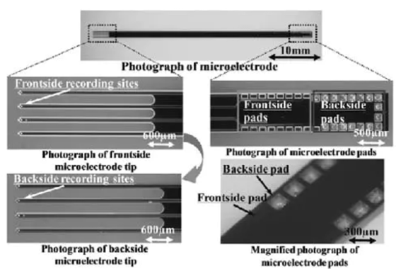
Fig2:Picture of Neuronode100 sample
Fig2 is an enlarged picture of Neuronode100 sample. Output pads for bonding to external device are arranged at the end of the microelectrode. The Neuronode100 is fabricated by applying standard photolithography in bulk micromachining process.
More info: info@t-microtec.com

English Site Menu
Company
Technology
Foundry service
Service case study