T-Micro 3D-Stacking LSI process technology
Fine-pitch Micro-TSV:

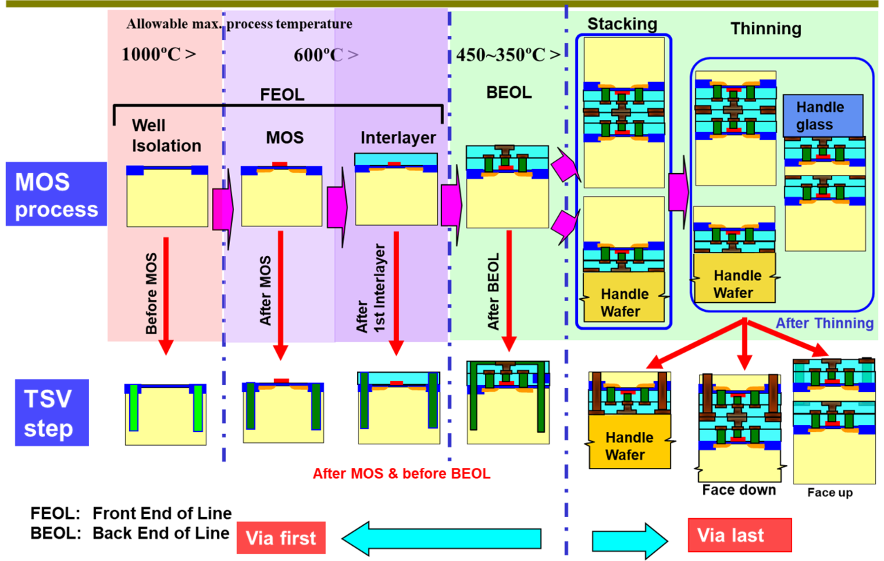
When the TSV is formed after the MOS device is formed, the suitable conductor materials are tungsten. Further, when the TSV is formed after the front-end-of-line (FEOL) process is completed, the suitable conductor materials are tungsten, copper, etc.
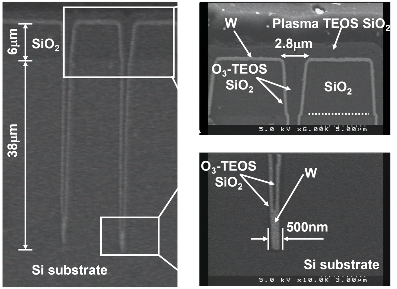
During the TSV formation process, it is important to fabricate sidewall insulator, a contact and barrier metal of TSV with a high aspect ratio at a low temperature. Fig-2 shows SEM images of T-micro’s fine-pitch μ-TSV. The insulator layer is formed by means of O3-TEOS CVD. The conformal silicon dioxide layer is obtained via reaction that occurs at the silicon surface at a relatively low temperature (-350℃)

English Site Menu
Company
Technology
Foundry service
Service case study

