T-micro 3D-Stacking LSI process technology
https://www.t-microtec.com/category/1420389.html
Overview:
Based on Moore’s law, 2-D(two-dimensional) semiconductor integration technology has expanded rapidly over the past three decades due largely to the good scalability of MOS devices. In recent years, however, operation voltage scaling causes nonconformity to the ideal scaling theory. The value of k T/q, which defines the minimum subthreshold swing of MOS transistors, does not scale down. Actually, the subthreshold leakage increases as the threshold voltage (Vth) of MOS transistors decreases. Since the subthreshold leakage surpasses the junction leakage in the recent MOS devices that have high current drivability, it becomes more and more difficult to lowering Vth of MOS transistors while ensuring low leakage current. It results in trade-off between power and performance.
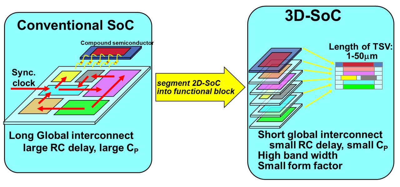
These days 3-D (three-dimensional) LSI is expected as a good solution for the challenge and the development of 3-D large-scale integration (3D-LSI) technologies has accelerated and has advanced from a research level to a pre-mass production level. As shown in Fig-1: Advantaged of 3D System-on-Chip (SoC), the 3D SoC is configured as segmenting 2D SoC into functional blocks, stacking these blocks, and interconnecting them with short signal paths.
3D-Stacking LSI devices can have high energy efficiency, small form factor, heterogeneous integration, and the capability to realize a new architecture, such as high-speed parallel data processing and multiple functions, at a low cost.
The 3D-Stacking LSI technology consist of several fundamental technologies: (1) through silicon via (TSV) formation, (2) bump formation, (3) wafer thinning, (4) chip/wafer alignment, and (5) chip/wafer stacking. Tohoku Micro Tec Co., Ltd. (T-micro) is the unique and advanced 3D-Stacking LSI process-oriented company, focusing on the above five fundamental technologies, and have a variety of patents related to the technologies in collaboration with Koyanagi Research Laboratory at Tohoku University.
The current 3D-Stacking LSI structure forms TSV under the peripheral bonding pads so that the through-hole dimension can be as large as the bonding pad size. Though this method can improve the form factor with minor 2D layout modification, measurable stress mismatch will occur between silicon and the conducting material in TSV. Furthermore, performance improvement by 3D-Stacking could be not enough due to huge register and load at thick TSVs.
In order for chip vendors to be satisfied with improvement of both form factor and performance by 3D-Stacking technology, it is essential that there is no restriction or limitation at inter-chip connection by TSV and bump. T-micro is thinking and focusing on that, for utilizing such a fully-flexible 3D-Stacking LSI, TSV and bump pitch must be reduced less than 5 μm as well as TSV diameter should be reduced to less than 2 μm. It results in that all and any functional blocks in a stacked chip can be directly connected to any layer by more than ten thousand TSVs without chip area penalty. T-micro’s unique and advanced 3D-Stacking LSI process technology utilizes such micro-TSVs and micro-bumps in the current and general CMOS process.
More info: info@t-microtec.com

English Site Menu
Company
Technology
Foundry service
Service case study