Au Micro Cylinder Bump

Au cylinder bump is T-Micro's uniuqe micro-bump technology. Now T-Micro provides Au micro cylinder bump process service to world-wide customers from only one-wafer. Au cylinder bump supports both one bump/one connection and multiple bumps/one connection so that electrical connectivity yield becomes higher than standard Au bump.

(Au cylinder bump spec)
- Size >3.5um diameter (Design-able)
- Pitch >7um
- Height <3um (Design-able)
- Au wall thickness ~100nm

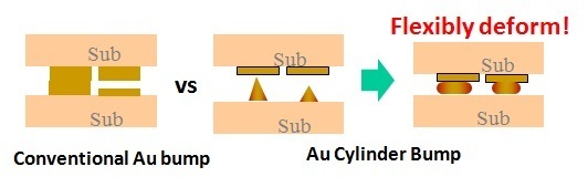
Au cylinder bump is hollow and formed by thin Au wall and Au base.

1) Bump size and shape scalability

Au cylinder bump's size and shape are design-able based on client's spec.

2) Large bonding margin

Since Au cylinder bump's inside is hollow, it well deforms at bonding. 

Au cylinder deformation.jpg

お問合せ・ご相談はこちら

お電話でのお問合せ・ご相談はこちら
022-398-6264

担当:元吉

T-Micro is the unique and advanced 3D/2.5D IC process and MEMS process-oriented company, originated in Tohoku University.
As an exclusive technical representative of GINTI "Global Integration Initiative" facility, we provide worldwide customers with 3D/ 2.5D/ MEMS full foundry service as well as partial process service by use of a complete line of state-of-the-art 200 and 300mm equipment in a cost-effective and short-TAT way for R/D, prototype, and small volume production.

東北マイクロテック(T-Micro)は、最先端の積層型三次元IC(3D-IC)技術をベースにした会社で、微細TSV(貫通配線)、マイクロバンプ接合等の新技術を入れ、今後のIT需要の拡大に呼応して、従来のICチップに高性能・高機能・小型化・省電力化といった新しい機能を付加します。新規の積層型センサの開発と並行してお客様に以下のサービスを提供致します。

  1. 数㎜角のチップから12インチウェハレベルの加工が可能で、お客様の3D-ICやMEMSのプロトタイプ試作、部分試作サポート、材料・装置評価用サンプル試作、少量生産をサポートします。
  2. 半導体微細加工技術及びMEMS製造技術をベースにバイオエレクトロニックデバイスの試作をサポートします。

弊社の技術・サービス、ホームページの内容に御意見やお問い合わせがございましたら、お気軽にご連絡ください。