
Optical Waveguide - integrated Si Brain Probe Mfg service
Neuronode800 :
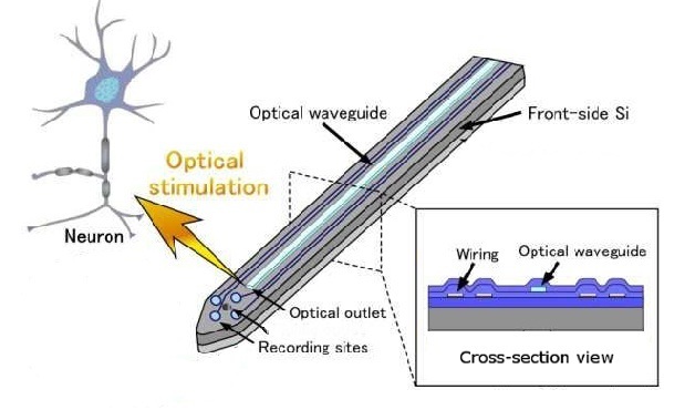
Neuronode800 series are the Optical Waveguide-integrated Si micro brain probe for brain signal recording / stimulation of Optogenetics study developed for a custom project.
Specification :
Probe material : Si (Silicon)
Probe length : 5, 10, 20, 33 mm or Custom
Probe thickness : 40 um
Probe width : 160 um (200 um for 32ch) at 1 ch optical waveguide
Electrode site material : Ir (Pt or Au optional)
Electrode site layout : Tetrode 4ch, Laminar 32 ch or Custom
Electrode site diameter : 10, 15 um or Custom
Optical waveguide dimension : 2.5 x 15 um (core & clad)
Optical waveguide outlet angle : 90 or 22.5 degree or Custom
Optical waveguide channel number : up to 8
Package : Special Acute (PCB). Special implantable package is negotiable.
Overview :
Optical waveguide consists of Silicon Nitride and Silicon Oxide. It is integrated between metal wiring leads on a front surface of Silicon substrate.
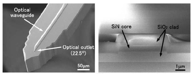
Core of Silicon Nitride is around 800 nm thick, and clad of Silicon Oxide is around 15 um wide by 800 nm thick at upper and lower layer respectively. In total the optical waveguide dimension is 2.5 um x 15 um.
Electrode sites are located close to probe's tip in order to sense signals from Neurons stimulated by optical wave.
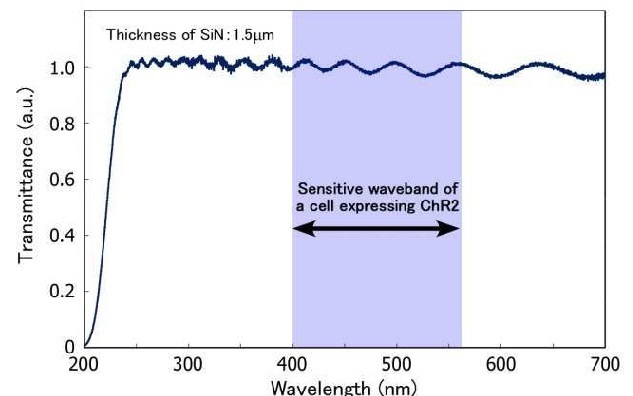
Transmission characteristics of our optical waveguide are shown as the above. The optical waveguide, integrated on Si probe, has enough high transimittance in sensitive waveband, 400 - 560 nm, of a cell expressing ChR2.
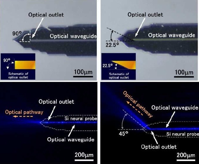
Neuronode800 supports two angles: 90-degree and 22.5-degree, of outlet of the optical waveguide integrated. Optical pathway at each angle from outlet of the optical waveguide is shown as the above. 90-degree outlet outputs straight pathway while 22.5-degree outputs 45-degree pathway. The picture of 22.5-degree is horizontal angle. Neuronode800 support 22.5-degree of vertical angle so that optical pathway goes at 45-dgree verticall angle to probe's front surface.
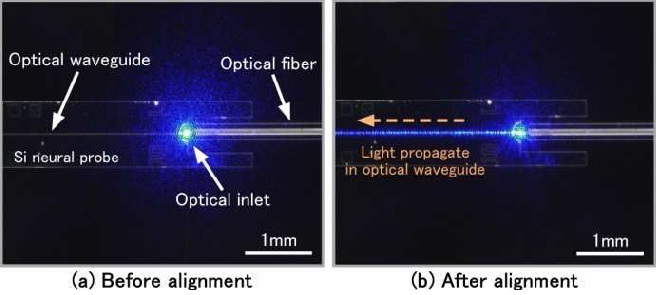
Precise alignment is required for connecting Si probe to optical fiber. As the above picture, no alignmnet causes light leakage. After alignment procedure, optical fiber is fixed with PCB board of Si probe. As the result, the leakgae is prevented and reduced as the above. Neuronode800's package is currently only special Acute type which can fix optical fiber based on position alignment.
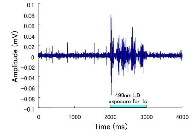
In-vitro experiments of optical stimulation of neurons in the hippocampal slice obtained from Thy1.2-ChR2-Venus rats was performed. Exposing and stimulating neurons to 490 nm wavelength lase diode light from outlet of Neuronode800 for 1 second, the Neuronode800 observed neuronal action potentials as the above.
Download : Neuronode800 catalog
More info: info@t-microtec.com
English Site Menu
Company
Technology
Foundry service
Service case study