
Process Facilities
We have 2 process facilities at Tohoku area, 300km north of Tokyo, in Japan for 3D/2.5D/MEMS foundry service.
1) Process for 12"/8" wafer: "GINTI" (facility name)
2) Process for 8"/6"/2" wafer: "Tohoku Univ facility"
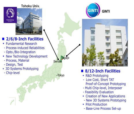
1) 12"& 8"Wafer process facility "GINTI"
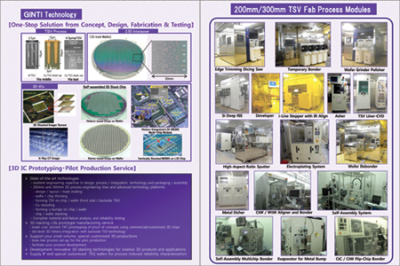
GINTI is the leading-edge 3D/2.5D/MEMS process facility started by Tohoku University to provide fabrication services to worldwide clients that are interested in developing new 2.5/3D design and integration technologies using micro TSV (Through Silicon Via) and micro bump.
Using the base technology originally developed at Tohoku University in Japan GINTI offers a broad range of 2.5/3D foundry services including:
i) Prototype processing by GINTI’s proprietary 3D stacking methodology “Chip-to-Wafer” using commercial/customized 2D chips,
ii) Full 200/300 mm wafer level processing,
iii) Prototype and Low volume production, and
ix) Creation of a 2.5/3D IC workflow and process methodology.
GINTI's cost-competitive process development infrastructure, using a complete line of state-of-the-art equipment, provides clients with a cost-effective and short-term TAT prototyping service for “proof of concept” projects, and a base-line process set-up service for 2.5/3D IC pilot production.
Tohoku Microtec (T-micro) is a strategic partner of GINTI and GINTI's exclusive representative of 2.5/3D IC process service business in the world-wide. T-micro's process engineers are operating and maintaining a complete line of the most advanced 200/300 mm equipment in GINTI facility. Further, T-micro's design engieers always consult 2.5/3D design methodology for GINTI's clients.
Please click here for more details of GINTI !
2) Tohoku univ. process facility for 2"/6"/8" wafer
Chip-to-Chip (CtC) process needs flexible prcoess flow which includes more complicated steps and sometimes needs a small Si support wafer and handling tools. This facility has a long history of advanced and challenging process step developments for many research projects. These days MEMS development projects are going up. This facility presents great performance for their 6" wafers in terms of processing costs, TAT, and process quality.

English Site Menu
Company
Technology
Foundry service
Service case study