Partial process service

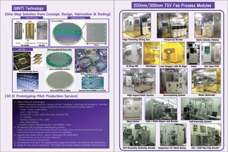
By use of our new, complete, and cost-competitive 3D-IC/Si-Interposer/MEMS line of 200/300 mm wafer with state‐of‐the‐art equipments such as:
- Lithography (i-line stepper with IR alignment)
- Si/SiO2 deep etch

- CVD (TSV liner)
- Sputter
- Electroplating
- Metal etch
- Temporary bonding
- Temporary debonding,

We provide worldwide customers with a cost‐effective and short‐term TAT partial process service as below:

- Wafer thinning,

- TSV making,

- Si/SiO2 deep trench,

- Bump formulation,

- RDL (Cu damascene is available),

- Bonding, etc.

お問合せ・ご相談はこちら

お電話でのお問合せ・ご相談はこちら
022-398-6264

担当:元吉

T-Micro is the unique and advanced 3D/2.5D IC process and MEMS process-oriented company, originated in Tohoku University.
As an exclusive technical representative of GINTI "Global Integration Initiative" facility, we provide worldwide customers with 3D/ 2.5D/ MEMS full foundry service as well as partial process service by use of a complete line of state-of-the-art 200 and 300mm equipment in a cost-effective and short-TAT way for R/D, prototype, and small volume production.

東北マイクロテック(T-Micro)は、最先端の積層型三次元IC(3D-IC)技術をベースにした会社で、微細TSV(貫通配線)、マイクロバンプ接合等の新技術を入れ、今後のIT需要の拡大に呼応して、従来のICチップに高性能・高機能・小型化・省電力化といった新しい機能を付加します。新規の積層型センサの開発と並行してお客様に以下のサービスを提供致します。

  1. 数㎜角のチップから12インチウェハレベルの加工が可能で、お客様の3D-ICやMEMSのプロトタイプ試作、部分試作サポート、材料・装置評価用サンプル試作、少量生産をサポートします。
  2. 半導体微細加工技術及びMEMS製造技術をベースにバイオエレクトロニックデバイスの試作をサポートします。

弊社の技術・サービス、ホームページの内容に御意見やお問い合わせがございましたら、お気軽にご連絡ください。