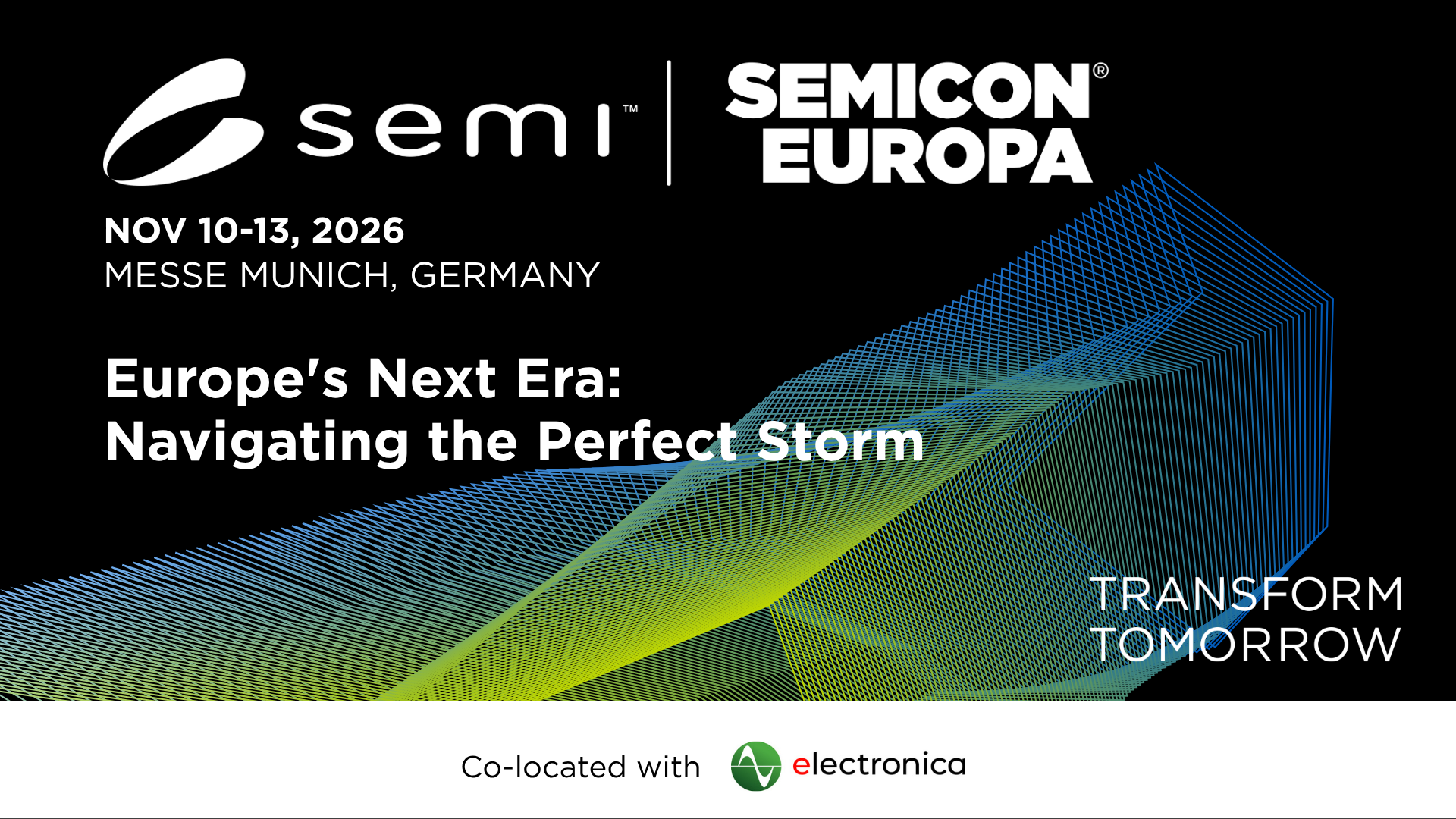
Tohoku Microtec Co., Ltd. (T-Micro) will participate in SEMICON Europa 2026, taking place at Messe München in Munich, Germany, from November 10 to 13, 2026.
Held alongside electronica, SEMICON Europa brings together companies and research organizations across the semiconductor and electronics industries. The event provides a meeting place for discussing advanced packaging, emerging technologies, and international collaboration.
T-Micro will exhibit at the Miyagi Prefecture joint booth, C1140 in Hall C1, together with the Micro System Integration Center (µSIC) at Tohoku University and Ball Wave.
We will introduce our 3D/2.5D-IC foundry capabilities, covering integration from individual chips to wafers up to 12 inches in diameter. Our technologies include through-silicon vias (TSVs), micro-bumps, wafer thinning, bonding, molding, and heterogeneous stacking.
By combining these processes, we help customers explore new device architectures and develop prototypes for advanced semiconductor integration.
Engineers, researchers, and development teams are invited to meet us in Munich to discuss their projects and processing requirements.
Exhibition Details
- Event: SEMICON Europa 2026
- Dates: November 10 (Tuesday)–November 13 (Friday), 2026
- Venue: Messe München, Munich, Germany
- Exhibition Area: Miyagi Prefecture Joint Booth
- Booth No.: C1140 — Hall C1
- Co-located Event: electronica 2026
Advance Consultation
Planning a technical discussion during the exhibition? Please contact us in advance with a brief description of your project, relevant processing requirements, and preferred meeting time.
Topics we welcome include:
- Development and prototyping of 3D/2.5D-IC devices
- TSV formation, redistribution layers (RDLs), and bump fabrication
- Chip-to-chip, chip-to-wafer, and wafer-to-wafer integration
- Wafer thinning and bonding
- Silicon interposer fabrication and heterogeneous integration
- Fine-pitch connections using gold micro-bumps
Examples of Our Technologies
1️⃣ 3D/2.5D-IC Integration
Our foundry services bring together TSVs, RDLs, micro-bumps, and bonding processes to support interconnected and stacked semiconductor devices. Customers can consult us about individual processing steps or a broader fabrication sequence.
2️⃣ TSV and Micro-Bump Technologies
We offer TSVs in a range of sizes and structures, along with multiple bump technologies. We welcome discussions about suitable interconnection approaches for your device design and development objectives.
3️⃣ Wafer Processing and Prototype Fabrication
Our processing capabilities extend from individual dies to 12-inch wafers. Services include thinning, bonding, and other fabrication steps needed to prepare and integrate semiconductor prototypes.
4️⃣ Heterogeneous Integration and Fine-Pitch Bonding
We support projects that combine different chips and device functions. Our capabilities include gold micro-bump interconnections and silicon interposer fabrication for advanced integration research and development.
Links
- SEMICON Europa 2026 — Official Website
- T-Micro — SEMICON Europa 2026 Exhibitor Profile
- Tohoku Microtec — Official Website
- Contact T-Micro
Join us at Booth C1140, Hall C1, in Munich—we look forward to discussing your next development project!