
We attend ECTC2016 !!
May 31-June 3, 2016. Conference & Exhibition
ECTC2016 (IEEE Electronic Components and Technology Conference), Booth No.219
Las Vegas, NV
http://ectc.net/
See you at ECTC2016!!
May 31-June 3, 2016. Conference & Exhibition
ECTC2016 (IEEE Electronic Components and Technology Conference), Booth No.219
Las Vegas, NV
http://ectc.net/
See you at ECTC2016!!
Good meeting you at No 1232 in SemiconWest 2015 during July 14-16 !!
We announced our new patented Micro Au Cone Bump technology.
Technology: Micro Au-Cone Bump
Bump size: 2.5um x 2.5um
Bump Pitch: 5 um (Minimum)
Material: Au
Target Application: Sensors (Compound, X-Ray, SOI, etc)
For detailed information, please contact hasegawa@t-microtec.com (San Jose CA)
T-Micro attends 3D-ASIP 2014 !!
3D Architectures for Semiconductor Integration and Packaginghttp://www.3dasip.org/
December 10-12, 2014Burlingame, CA
We have a table-booth, please join us !!
Please visit our booth at the following conference & exhibition in November 2014 !!
Nov 15 - 19, 2014. Conference & ExhibitionNeuroscience 2014
Booth No. 1913Washington D.C.
http://www.sfn.org/annual-meeting/neuroscience-2014
T-Micro presents Omni-directional Brain probe for Deep brain recording & Stimulation !
Nov 12 - 13, 2014. Conference
T Sensors Summit for Trillion Sensor Roadmap
San Diego CA
http://www.tsensorssummit.org/
T-Micro presents 3D-IC/Si Interposer/MEMS foundry service by GINTI's 200/300mm wafer process line.
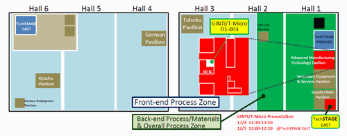
Thank you so much for visiting T-Micro and GINTI (Global Integration Initiative: http://www.ginti.niche.tohoku.ac.jp ) booth at Semicon Japan 2013 !
(Semicon Japan ) http://www.semiconjapan.org
Dec.4-Dec.6, 2013
Makuhari Messe, Chiba, Japan
Booth: Hall 1, D1-003
Dec. 4 12:30~12:50
Dec. 5 12:00~12:20 (Release Presentation)
Location:
Thank you for visiting T-micro/GINTI booth at IEEE International 3D Integration Conference 2013 in San Francisco, CA, USA on Oct 2-4, 2013.
T-micro/GINTI team exhibited the brand-new "Global Integration Initiative" activity, which is 3D/2.5D IC process service with a complete line of 200 and 300mm equipments as one stop-service of TSV design, mfg, pkg and test for R/D, prototype, and small volume production.
GINITI specilizes Wafer on Wafer, Chip on Chip as well as Chip on Wafer, which stack multiple layers of a variety of 2D conventional KGDs (Known Good Die) on a support wafer.
More details of GINTI. Please click here !
T ohoku-MicroTec (T-Micro) was participating in 42nd INTERNEPCON JAPAN !!
Jan. 16-18, 2013 10:00-18:00 (10:00-17:00 on Jan. 18) , Tokyo Big Sight, Japan
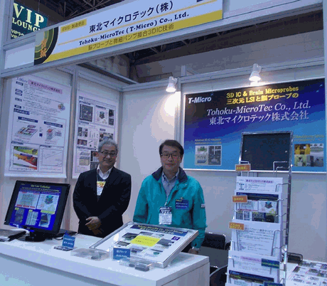
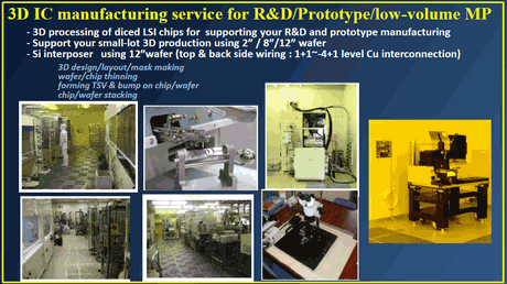
We presented about (1)3D IC demo chips, (2) Several type of Barain microprobes for neuroscience, and (3) 3D IC manufacturing service.
We can make 3D stack chip using diced LSI chips. And 3D processing using 8"/12" LSI wafer and 12" Si interposer with high aspect ratio TSV (up to 10) will be availavle from this April.
Oct 10, 2012 : Press-Release
Tohoku-MicroTec Co., Ltd. forges strategic alliance with Microprobes for Life Sciences (Gaithersburg, MD, USA) to offer multichannel silicion nerual interfaces.
Tohoku-MicroTec attend Neuroscience2012 !!
See you at our booth in Neuroscience2012.
Oct 13 - 17, 2012
Ernest N. Morial Convention Center, New Orleans
Booth: 1735
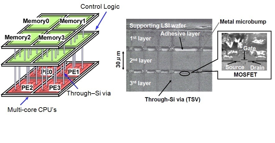
3D-stacked LSI is the next generation device which is expected to reduce power consumption down to half. From the view of clean environment, establishment of stable, secure and cost-effective technology of 3D stacked LSI is these days craved for. In anticipation of substitution for the current 2D LSI and promotion of the 3D-stacked LSI in a variety of market segments, further research and development are essential.
Tohoku-MicroTec Co., Ltd. (Tohoku-MicroTec), established at Sendai, Japan in April, 2010, is the unique and leading 3D-Stacked LSI process-oriented company, utilizing the next generation process & manufacturing technology, originated in Tohoku university, of fine-pitch Through-Silicon-VIA (TSV), Microbump, Thinning, Bonding and Alignment.
In wide and tight collaboration with New Industry Creation Hatchery Center of Tohoku University, we research and develop Bio-Electronics products for Neuroscience, provide 3D-Stacked LSI prototype manufacturing services at a drastic cost-effective way, and counsel on the development related to 3D-Stacked LSI process.
T-Microtec opened its headquarter office at T-Biz building in Tohoku university.
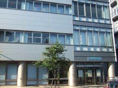
Headquarter address
6-6-40 Suite 203, Aza-Aoba, Aramaki, Aoba-ku, Sendai, Miyagi, 980-8579 Japan
Tel: +81-22-398-6264
(022-398-6264 in Japan)
Fax: +81-22-398-6265
(022-398-6265 in Japan)
E-mail: info@t-microtec.com
Company
Technology
Foundry service
Service case study