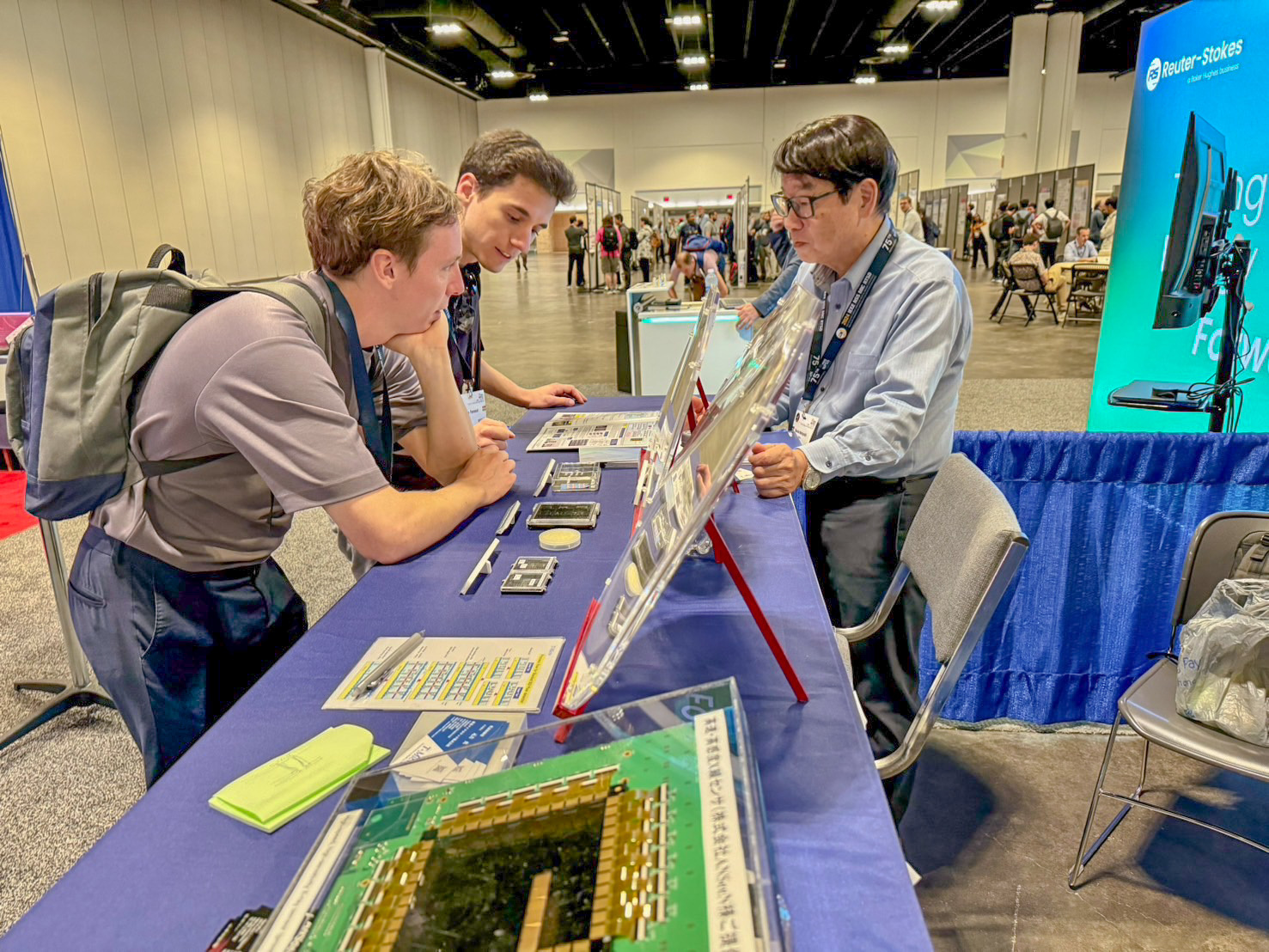
Tohoku Microtec Co., Ltd. (T-Micro) will participate in the 3rd Semiconductor Technology Expo in Kyushu, Japan, taking place at Marine Messe Fukuoka on September 30 and October 1, 2026.


 The exhibition brings together technologies and services across the semiconductor supply chain, covering design, manufacturing equipment, components, materials, inspection, and measurement.

It provides opportunities for semiconductor companies and research institutions, particularly those in the Kyushu region, to exchange ideas, explore partnerships, and discuss business opportunities.


 As a foundry supporting 3D-IC research and prototype development, T-Micro will showcase its processing and integration capabilities, including through-silicon vias (TSVs), redistribution layers (RDLs), and microbump bonding.

We welcome discussions on prototyping with customer-supplied IC chips and wafers, silicon interposers, heterogeneous device stacking, and other development challenges.


 We look forward to discussing your projects and technical requirements with you. Please visit us at Booth B6-8 in Hall B!


 Exhibition Details

  • Event : The 3rd Semiconductor Technology Expo in Kyushu, Japan
  • Dates:September 30 (Wednesday) – October 1 (Thursday), 2026
  • Opening Hours:10:00–17:00 on both days
  • Venue : Marine Messe Fukuoka, Halls A and B, Fukuoka, Japan
  • T-Micro Exhibition Location:Hall B
  • Booth No.:B6-8
  • Admission:Free with advance visitor registration


 Advance Consultation

 If you have a prototype project in mind or a processing challenge you would like to discuss, we welcome inquiries before the exhibition.
Sharing your requirements and preferred meeting time in advance will help us prepare for a productive discussion at our booth.

Please send your inquiry through our Contact Form.


 Topics we can discuss include:

  • Prototyping for 3D-IC and 2.5D IC development
  • Individual processing steps, including TSV fabrication, RDL formation, and bumping
  • Chips stacking and heterogeneous integration using existing IC chips
  • Fine-pitch chip-to-chip connections with gold microbumps
  • Silicon interposer and chiplet-related prototyping
  • Sample fabrication for materials and equipment evaluation
     

 Technologies and Services on Display

1️⃣ 3D-IC and 2.5D IC Prototyping

 We support the development of stacked devices and high-density packaging through TSV, RDL, and microbump technologies. Our services range from individual processing steps to prototype fabrication involving multiple integrated processes.

2️⃣ Contact Wafer and Chip Processing

 Our processing capabilities cover IC chips measuring just a few millimeters on each side through to wafers up to 12 inches in diameter. We welcome inquiries involving deposition, photolithography, etching, chemical mechanical polishing (CMP), bonding, and chip assembly, tailored to your prototyping and evaluation needs.

3️⃣ Heterogeneous Integration and Chiplet Prototyping

 We help customers combine devices with different functions and develop 3D structures using their own IC chips. We also welcome discussions on silicon interposers and chiplet-related prototypes, based on your intended device architecture and development objectives.

4️⃣ Gold Mcrobump Bonding

 We will introduce gold microbump technologies for fine-pitch connections. Visit our booth to discuss bonding approaches for high-density sensor interconnections and stacked semiconductor devices.


For more details, please visit our SEMICON Taiwan 2026 exhibitor profile.


 Links
 Our sincere thanks to everyone who visited the Tohoku-MicroTec Co., Ltd. (T-Micro) display at the Miyagi Prefecture / Sendai City booth in the Japan Pavilion during SEMICON Taiwan 2026, held in Taipei, Taiwan, on September 2–4, 2026.


 It was a pleasure to meet you in person and introduce our technologies and processing capabilities, including:

  • 3D-IC and 2.5D IC technologies
  • Through-silicon via (TSV) processing
  • Redistribution layer (RDL) fabrication
  • Bump formation


 We hope to build on these connections through future collaboration, helping you address your technical challenges with technologies and services that support semiconductor prototyping and development.

 We welcome further questions about our exhibits, as well as inquiries regarding 3D integration, silicon interposers, heterogeneous device stacking, and chiplet prototyping.
Whether or not you were able to attend, we would be happy to discuss your needs through the inquiry form below.


 Thank you for your continued support of T-Micro.
Form : Contact Form


We look forward to seeing you again!


 Links

 Tohoku Microtec Co., Ltd. (T-Micro) is delighted to announce its participation in SEMICON Taiwan 2026, taking place in Taipei, Taiwan, from September 2 to 4, 2026.


 SEMICON Taiwan is an international exhibition connecting companies across the semiconductor supply chain, including equipment, materials, components, and inspection technologies.

The event offers opportunities to share technical developments, explore collaboration, and discuss business needs with industry professionals from around the world.


 T-Micro will join the Miyagi Prefecture / Sendai City joint booth within the Japan Pavilion.

As a foundry focused on 3D-IC development and prototyping, we will showcase technologies and services supporting semiconductor research and advanced integration.


 Our capabilities include processing customer-supplied IC chips and wafers up to 12 inches in diameter using through-silicon vias (TSVs), redistribution layers (RDLs), and bumping technologies.

We also support prototyping for silicon interposers, heterogeneous stacked devices, and chiplets.

Further information is available on our official exhibitor profile.


 We welcome the opportunity to discuss your projects and technical challenges with engineers, researchers, and industry partners from Taiwan and beyond.

Visit us at Booth Q6134 to explore how T-Micro can support your development needs.


 Exhibition Details

  • Event : SEMICON Taiwan 2026
  • Dates:September 2 (Wednesday)–September 4 (Friday), 2026
  • Venue : Taipei Nangang Exhibition Center (TaiNEX 1 & 2), Taipei, Taiwan
  • Exhibition Area:Japan Pavilion — Miyagi Prefecture / Sendai City Joint Booth
  • Booth No.:Q6134 


 Advance Consultation
 
If you would like to discuss a specific project during the exhibition, we encourage you to contact us beforehand.
Sharing your technical requirements, development goals, and preferred meeting time will help us prepare for a productive conversation.

 Contact Form : 
https://www.t-microtec.com/17749130183965

 Potential discussion topics include:

  • Prototyping and development for 3D-IC and 2.5D IC applications
  • Chip-level stacking and heterogeneous integration
  • Contract processing for TSVs, RDLs, and bumps
  • Fine-pitch bonding with gold micro-bumps
  • Silicon interposer and chiplet prototyping
  • Device prototypes and evaluation samples for R&D projects 
     

 Examples of Our Technologies

1️⃣ 3D-IC and 2.5D IC Technologies

 We combine TSV, micro-bump, and redistribution technologies to support the development of high-density semiconductor integration and stacked devices.

2️⃣ Wafer Processing and Prototyping Services

 Our services cover individual IC chips and wafers up to 12 inches in diameter. We welcome discussions about processing requirements for research, prototype fabrication, and evaluation.

3️⃣ Chip-Level 3D Integration

 We support the stacking of customer-supplied IC chips, including prototyping projects involving heterogeneous devices and chiplets.

4️⃣ Fine-Pitch Gold Micro-Bump Interconnection

 We will present our gold micro-bump bonding capabilities for closely spaced chip connections and discuss their application to heterogeneous device integration.


For more details, please visit our SEMICON Taiwan 2026 exhibitor profile.


 Links

We look forward to welcoming you to Booth Q6134 in Taipei!

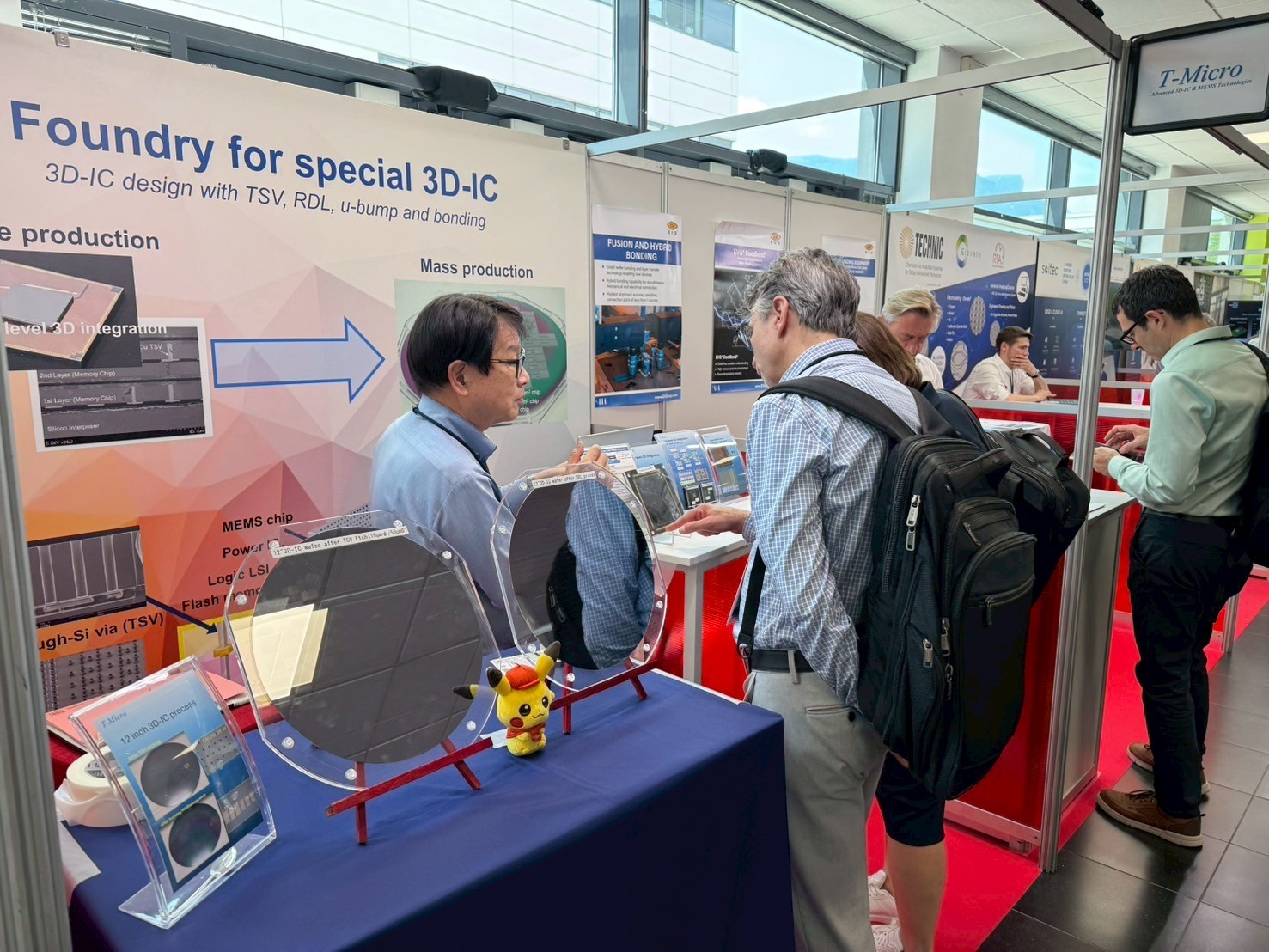
 We would like to express our sincere appreciation to everyone who visited the Tohoku-MicroTec Co., Ltd. (T-Micro) booth at CEA-Leti Innovation Days / LID World Summit 2026, held in Grenoble, France.

We would also like to thank everyone who attended the presentation delivered by our President, Makoto Motoyoshi, during the “Shaping What’s Next” session.


 Throughout the event, we had valuable opportunities to exchange ideas with researchers, engineers, and industry professionals from around the world regarding our technologies and services, including:

  • 3D-IC and 3D/2.5D IC technologies
  • Fine-pitch interconnection using gold bumps
  • Chip-level 3D integration
  • Wafer processing services
  • Prototype development and contract R&D support

 We were delighted to introduce our technologies and services and to connect with so many people from across the global semiconductor and microelectronics community.

As a development-oriented foundry specializing in 3D-IC technologies, T-Micro will continue to enhance its technical capabilities and services to support advanced research and the realization of next-generation semiconductor technologies.

Thank you again for your interest and support.

For inquiries regarding our 3D-IC technologies, wafer processing, prototype development, or contract R&D services, please feel free to contact us through the inquiry form below.

Form : Contact Form


We look forward to seeing you again!


 Links

 Thank you very much for visiting our booth at SEMICON Southeast Asia 2026 in Kuala Lumpur.

We truly appreciate the valuable conversations and connections with so many of you.


We will continue to provide better products and services to support your business success.

Welook forward to continuing our partnership and exploring new opportunities together.


 If you have any follow-up questions about TEG wafers, deposition, or anything else we showcased, please feel free to reach out using the form below.

Form : https://www.t-microtec.com/17581502428702


 We look forward to seeing you again soon.


 Links


Tohoku Microtec Co., Ltd. (T-Micro) is pleased to announce that we will exhibit and give a presentation at CEA-Leti Innovation Days / LID World Summit 2026, to be held in Grenoble, France in June 2026.


 CEA-Leti Innovation Days / LID World Summit is an international event that brings together engineers, research institutions, startups, equipment and materials manufacturers, device manufacturers, and other key players in the semiconductor and microelectronics fields from around the world.


 The 2026 program will cover important technology areas for the future of the semiconductor industry, including semiconductor technologies for the AI era, advanced packaging, sustainable semiconductor manufacturing, and next-generation devices.


 At this year’s event, T-Micro will introduce its technologies and services as a development-oriented foundry specializing in 3D-IC. Our offerings include 3D-IC prototyping from 12-inch wafer-level to chip-level processes, fine-pitch interconnection using gold bumps, and chip-level 3D integration services.


 In addition, during the “Shaping What’s Next” session, our CEO, Makoto Motoyoshi, is scheduled to give a presentation titled “T-Micro's 3D-IC technology.”


 We look forward to meeting and speaking directly with visitors from Europe and around the world who are involved in semiconductors,advanced packaging, and research and development. Please feel free to visit us during the event.


 Exhibition Details


Presentation Information

  • Session:Shaping What's NextーMorning Session
  • Date and Time:June 25, 2026, 9:30-10:00
  • Speaker:Makoto Motoyoshi, CEO, Tohoku Microtec Co., Ltd.
  • Presentation Title:T-Micro's 3D-IC technology
  • ✅Note:
    During the event, T-Micro will introduce its 3D-IC-related technologies, contract prototyping services, and development support services.

    Although the presentation will be brief, we will provide a clear overview of our technical fields and initiatives. We encourage visitors to attend the presentation during their visit to the event.


 Advance Consultation
 To help make discussions on the day of the event more productive, we also welcome advance inquiries and consultation requests.

Please feel free to contact us through the form below. 

 Contact Form : 
https://www.t-microtec.com/17749130183965

 Examples of consultation topics:

  • Prototype development for 3D-IC and 3D/2.5D IC applications
  • Chip-level 3D integration
  • Fine-pitch interconnection using gold bumps
  • Wafer processing, microfabrication, and contract prototyping
  • Device prototyping and evaluation sample fabrication at the research and development stage
     

 Examples of Our Technologies

 1️⃣ 3D-IC/3D/2.5D IC Technologies
  …We will introduce high-density integration and stacking technologies for next-generation semiconductor packaging.

 2️⃣ Wafer Processing and Contract Prototyping Services 
  …We accept inquiries related to a wide range of technical challenges, from 12-inch wafer-level processes to chip-level processes, for research and development and prototype evaluation.

 3️⃣ Chip-Level 3D Integration

…We will introduce our prototype development and support services for chip-level 3D integration.

 4️⃣ Fine-Pitch Interconnection Using Gold Bumps

…We will introduce fine-pitch interconnection technologies using gold bumps, which support higher density and higher performance semiconductor devices.


 Links

Tohoku Microtec Co., Ltd. (T-Micro) is pleased to announce that we will exhibit at SEMICON Southeast Asia 2026, to be held in Kuala Lumpur, Malaysia in May 2026.


 Semicon Southeast Asia is an international exhibition that brings together key players from the semiconductor and electronics manufacturing supply chain, particularly across Southeast Asia.


 In recent years, investment in semiconductor manufacturing, back-end processes, electronic components, equipment, and materials has been accelerating across the Southeast Asian region.

We look forward to meeting and speaking directly with visitors who are interested in 3D-IC, Advanced Packaging, and Wafer Processing Technologies in the dynamic atmosphere of the event.


 At this year’s exhibition, T-Micro will present its technologies and services related to next-generation semiconductor packaging, including 3D-LSI technologies, at the NextGen Hub within the Innovation Booth.


 We warmly invite you to visit our booth and attend our presentation during the event.


 Exhibition Details

  • Event : SEMICON Southeast Asia 2026
  • Dates:May 5, 2026 - May 7, 2026
  • Venue : Malaysia International Trade & Exhibition Centre (MITEC), Kuala Lumpur, Malaysia
  • Booth No.:W1887 
  • ✅Note:Our booth will be located in the NextGen Hub within the Innovation Booth, Hall 1, 1F. Please feel free to stop by.


 Presentation Information

  • Date and Time:May 7, 2026, 11:40-11:55
  • Venue : NextGen Hub Stage
  • ✅Note:During the exhibition, T-Micro is scheduled to give a presentation at the NextGen Hub Stage.
    Although the presentation will be brief, we will provide a clear overview of our technical fields and initiatives. We encourage visitors to attend the presentation during their visit to the exhibition.


 Advance Consultation
 To help make discussions on the day of the event more productive, we also welcome advance inquiries and consultation requests.

Please feel free to contact us through the form below. 

 Contact Form : 
https://www.t-microtec.com/17749130183965

 Examples of consultation topics:

  • Contract wafer process services, including film deposition
  • Prototype development for 3D/2.5D IC applications


 Examples of Our Technologies

 1️⃣ 3D/2.5D IC Technologies
  …We will introduce high-density integration and stacking technologies for next-generation semiconductor packaging.

 2️⃣ Contract Wafer Deposition Services
  …We accept inquiries related to prototype development, process evaluation, and sample preparation for technical assessment, tailored to each customer’s specific technical challenges.

 3️⃣ Hybrid Bonding
  …
Hybrid bonding is an increasingly important technology area as semiconductor devices continue to advance toward finer geometries and higher levels of integration.


 Links

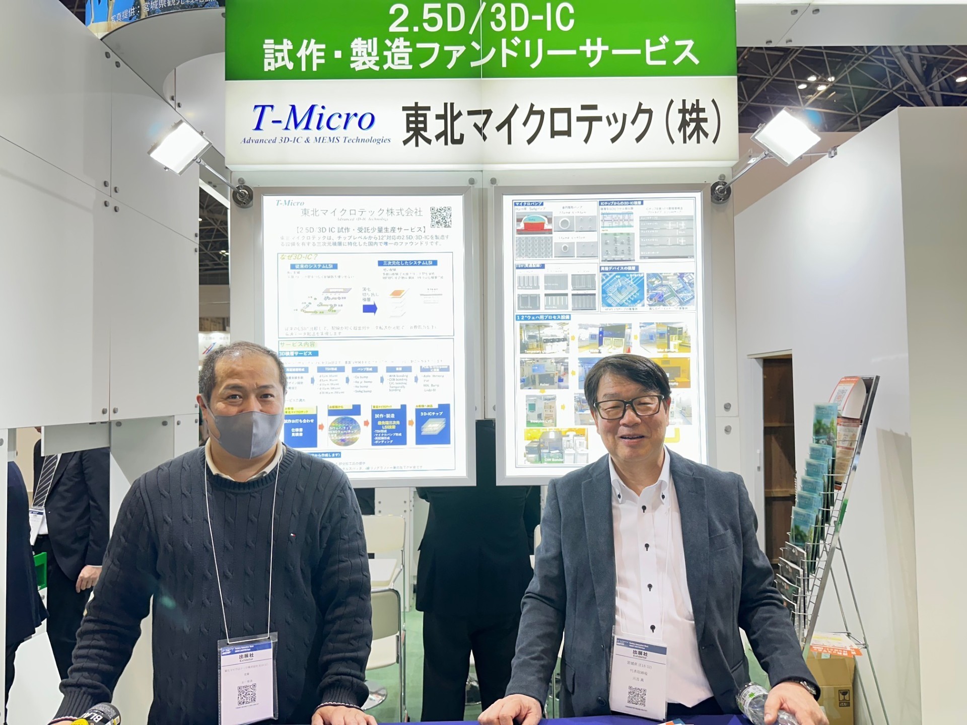
 Thank you very much for stopping by Tohoku Microtec Co., Ltd. (T-Micro) booth at the 40th NEPCON JAPAN (Miyagi Prefecture Joint Booth / Booth No. : E18-32).
 

 During the exhibition, we received many inquiries—especially regarding TEG wafers—and we truly appreciated the opportunity to hear about your background and challenges directly and discuss them with you.

 Below is a photo from our booth during the show.


 If you have any follow-up questions about TEG wafers, deposition, or anything else we showcased, please feel free to reach out using the form below.

Form : https://www.t-microtec.com/17581502428702


 We look forward to seeing you again soo.


 Links

 Tohoku Microtec Co., Ltd. (T-Micro) will exhibit at the 40th NEPCON JAPAN - Electronics Development & Implementation Exhibition in Tokyo, Japan, in January 2026.


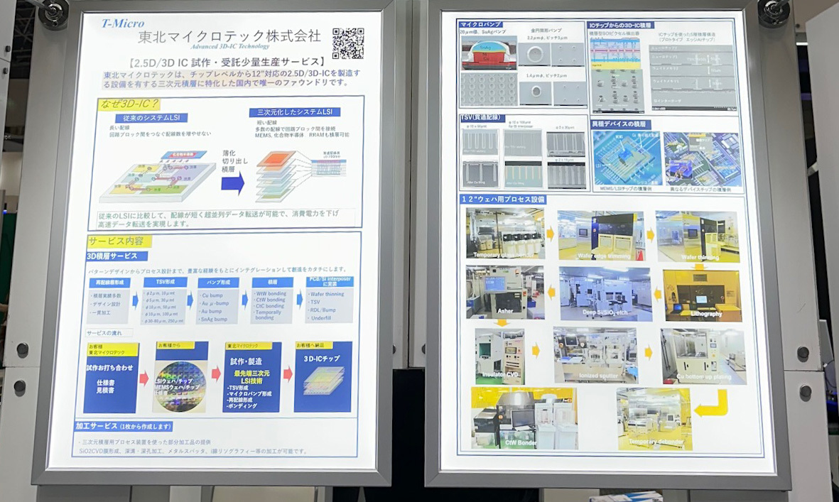
 Tohoku Microtec is a wafer process foundry supporting advanced semiconductor process development and packaging. We provide end-to-end support from wafer process to assembly, with a strong focus on 3D-IC (3D LSI) technologies.


 We look forward to meeting engineers and procurement professionals who are exploring practical solutions for advanced packaging, prototyping, and outsourced wafer process needs.


 Booth Information

  • Event : The 40th NEPCON JAPAN - Electronics Development & Implementation Exhibition
  • Date/Hours : January 21 (Wed) - 23 (Fri), 2026 / 10:00-17:00
  • Venue : Tokyo Big Sight (Tokyo, Japan)
  • Booth : E18-32, Miyagi Prefecture Joint Exhibition Booth
  • Note : The Miyagi joint booth is a collaborative initiative where local manufacturing companies showcase their technologies together. Please look for the "Tohoku MicroTec Co., Ltd." sign at the booth.


 Pre-meeting (Recommended)
 
To make discussions at the show smoother, we strongly recommend arranging a brief pre-meeting in advance.
Prease submit the contact form here, and our team will get back to you : 
https://www.t-microtec.com/17581502428702


 What we can discuss
 ❶ Outsourcing wafer processes (including thin-film deposition)
 ❷ 3D-IC prototyping cunsultation

 Our Technologies
 
❶ 3D-IC (3D LSI) packaging and assembly
 ❷ Contract wafer deposition services
 ❸ 12-inch wafer-ready thinning, bonding, molding, and heterogeneous material stacking/lamination
 

 Links / Contact

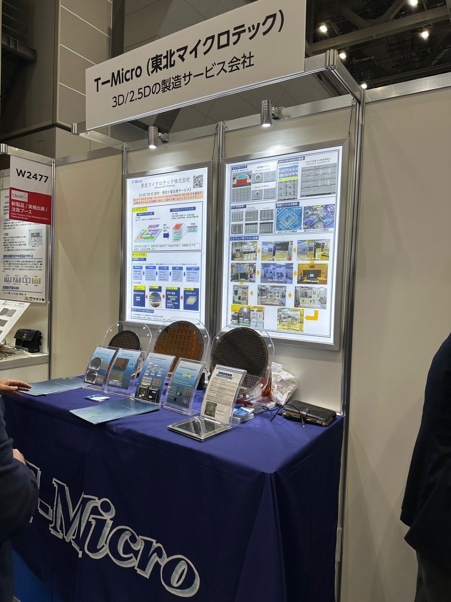
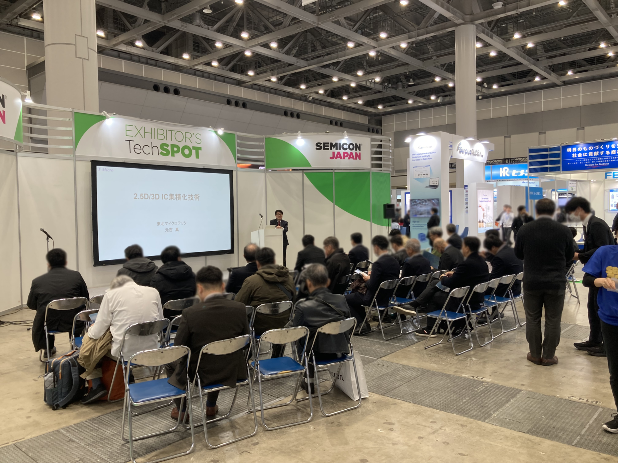
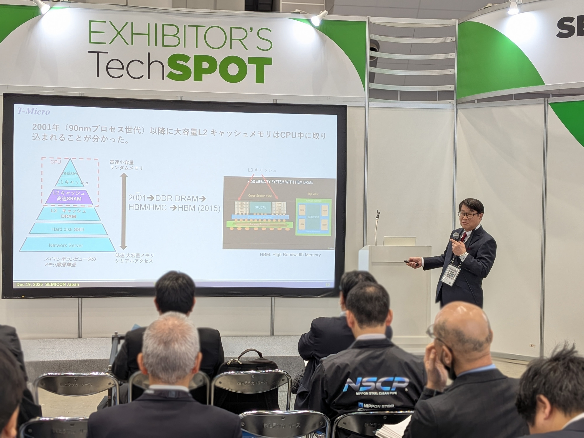
 Thank you for visiting our booth(W2477) and attending our seminar, "Evolution and Future Outlook of 3D/2.5D Technologies", at SEMICON Japan 2025.


 Tohoku-Microtec Co., Ltd. (T-Micro) was honored to welcome so many of you, and we truly enjoyed speaking with you.

During the show, we received many inquiries - especially around 3D/2.5D technology - and it was a pleasure to discuss your challenges and ideas in person.

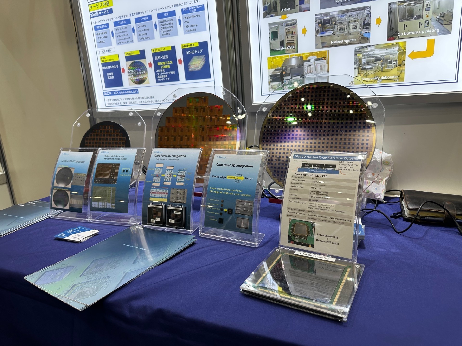
The attached photoes offer the glimpse of the lively atmosphere at our booth and seminar.


 If you would like to continue the discussion, please feel free to contact us via the inquiry form:

contact form


 We also look forward to seeing you at NEPCON JAPAN 2026 (Jan 21-23, 2026), where we plan to exhibit at the "Miyagi Prefecture booth".


Tohoku-Microtec Co., Ltd. (T-Micro)

 Tohoku Microtec Co., Ltd. will be exhibiting at SEMICON Japan 2025, to be held in Tokyo, Japan.
 

 SEMICON Japan 2025 is one of the largest semiconductor-related events in Japanーan international exhibition for electronics manufacturing that covers everything from semiconductor manufacturing technologies, equipment, and materials to SMART applications such as automobiles and IoT devices.


 On the day of the event, Tohoku Microtec engineer with over 20 years of experience in 3D technology development will give a presentation on how we started working on 3D technologies, how these technologies have evolved, and future trends.


 We will give a talk at the TechSPOT stage in West Hall 2 on Friday, Decemcer 19, 2025, from 11:30 to 11:50.

We will also have a booth in the TOUHOKU Pavilion (West Hall 2, booth W2477), so please feel free to stop by.


 Seminar Over view

  • Title : Evolution and Future Outlook of 3D/2.5D Technologies
  • Date & Time : Friday, December 19, 2025, 11:30-11:50
  • Location : TechSPOT, West Hall 2
  • Outline : Our engineer who has been engaged in 3D technology development for over 20 years will present how 3D technology development began, how it has progressed, and future trend.
  • Pre-event inquiry : Please contact us in advance via our contact form.


 Exhibit Overview

  • Dates : December 17(Wed) - December 19(Fri), 2025, 10:00-17:00
  • Venue : Tokyo Big Sight (Tokyo, Japan)
  • Booth : TOUHOKU Pavilion, West Hall 2, W2477
  • Pre-event inquiry : Please contact us in advance via our contact form.
  • ✅About T-Micro : We are a foundry specializing in advanced 3D-IC(3D-LSI) assembly, offering proprietary processes that enable integration from chip level up to 12-inch wafer level.

​
 What You'll See at Our Booth

 ❶ TSV Technology ー customizable sizes and structures for diverse device requirements.
 ❷ Micro-Bump Technology ー fine-pitch interconnects for high-density, low-resistance connections.
 ❸ Proceessing Technology ー thinning, bonding, molding, and heterogeneous stacking to maximize 3D integration freedom.


 Useful Links

 Contact

Tel : +81-22-398-6264

Email : info.tm@t-microtec.com


We look forward to meeting you in Tokyo!

 Tohoku Microtec Co., Ltd. will exhibit at SEMICON Europa 2025 in Munich, GermanyーEurope's largest semiconductor event.


 At our booth, we'll introduce our latest advances in 3D/2.5D-IC (3D-LSI) technologies.

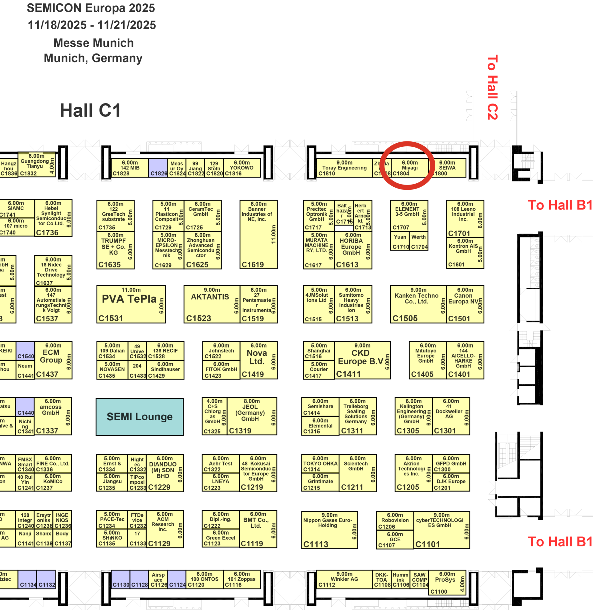
 Booth location : Hall C1, C1804ーupper-right area on the floor plan(marked with a red circle).
Please stop by and say  hello!

 Exhibit Overview

  • Dates : November 18(Tue) - November 21(Fri), 2025, 9:00-18:00
  • Venue : Messe München(Munich, Germany)
  • Booth : Hall C1, C1804
  • Pre-event inquiry : Please contact us in advance via our contact form.
  • ✅About T-Micro : We are a foundry specializing in advanced 3D-IC(3D-LSI) assembly, offering proprietary processes that enable integration from chip level up to 12-inch wafer level.

​
 What You'll See at Our Booth

 ❶ TSV Technology ー customizable sizes and structures for diverse device requirements.
 ❷ Micro-Bump Technology ー fine-pitch interconnects for high-density, low-resistance connections.
 ❸ Proceessing Technology ー thinning, bonding, molding, and heterogeneous stacking to maximize 3D integration freedom.


 Useful Links

 Contact

Tel : +81-22-398-6264

Email : info.tm@t-microtec.com


We look forward to meeting you in Munich!

 Tohoku Microtec Co., Ltd. will attend IEEE NSS/MIC/RTSD 2025 in Yokohama as visitors. 

 This international conference brings together researchers and industry to share the latest advances in nuclear science, medical imaging, and room-temperature semiconductor detectors.
The event will be held at Pacifico Yokohama North.

 We will be on site to gather semiconductor-related information and engage with stakeholders.

 If you would like to discuss our 3D-IC (3D LSI) capabilities during the event, please feel free to contact us in advance.

Event Overview

  • Dates: November 1–8, 2025, 8:00–18:00 (JST)

  • Venue: Pacifico Yokohama North

  • Pre-event consultation: Contact Form – https://www.t-microtec.com/17581502428702

  • Notes: We offer advanced packaging and micro-fabrication for 3D-IC (3D LSI), including micro-TSV and micro-bump, as well as contract manufacturing/prototyping and foundry services.

Links


 Tohoku Microtec Co., Ltd. will exhibit at the 2nd [Kyushu] Semiconductor Industry Exhibition to be held in Japan.

 The [Kyushu] Semiconductor Industry Exhibition is a trade show hosted at Marine Messe Fukuoka (Fukuoka City, Fukuoka Prefecture).
It is billed as "Kyushu's first specialized exhibition dedicated to the semiconductor industry."

 On the day of the event, we will introduce Tohoku Microtec's latest technologies related to 3D-IC (3D LSI).
We will exhibit at Booth B9-33 - please feel free to drop by!


 Exhibit Overview

  • Dates                   : October 8 (Wed) - October 9 (Thu), 2025, 10:00-17:00
  • Venue / Booth     : Marine Messe Fukuoka, Hall B / Booth B9-33
  • Pre-event inquiry : Contact Form
  • Note                     : We provide contract manufacturing, prototyping, and foundry services for 3D-IC (3D LSI) advanced packaging and micro-fabrication (e. g., micro-TSV, micro-bump). Please feel free to contact us.


Links

2025 CEA-Leti Innovation Days / LID World Summit
Jun. 17-19 @Grenoble, France

Dear Sir/Madam,

Thank you very much to everyone who visited our booth at the LID World Summit.
If you have any questions about our technology or business model, please feel free to contact me.
[info.tm@t-microtec.com]

We would also like to express our sincere gratitude to the Leti staf for their kind support.
We look forward to seeing you again next year.

Best Regards,
Makoto Motoyoshi (CEO)

Dear Sirs,

We are planning to attend at The 6th International Conference on Machine Learning and Intelligent Systems (MLIS 2024).
Let's discuss about the technological advances in the field of machine learning and intelligent systems there.

Nov 17 - 20 @Kampar, Perak, Malaysia

Home page - MLIS2024

See you at MLIS 2024!

2024 IEEE NSS MIC RTSD
Oct. 26th-Nov. 2nd @TAMPA, FLORIDA, USA

Dear Sir/Madam,

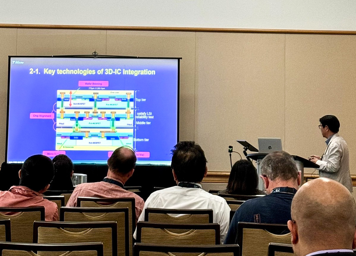
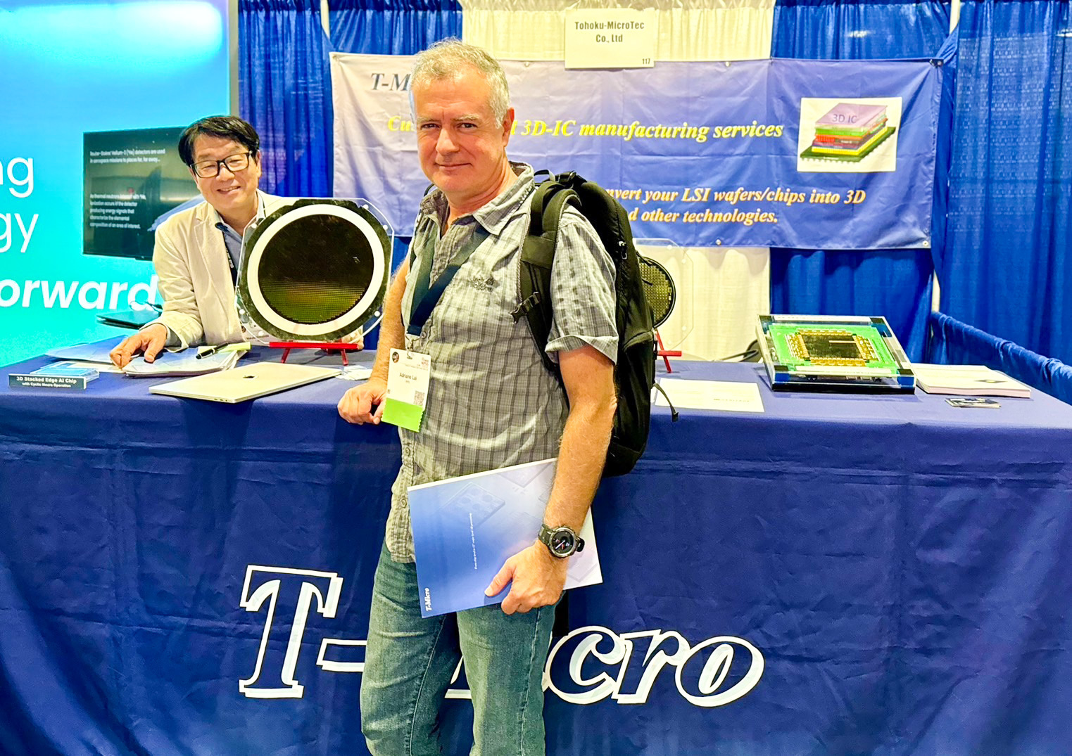
Thank you for visiting us at 2024 IEEE NSS MIC RTSD.

We presented our various 3D-ICs using elemental technologies such as TSV, stacking, micro bumping, etc.
In addition, our proprietary high-speed, high-precision chip positioning and micro bumping technologies were introduced. 

Of course, we exhibited our 3D-IC Technology with samples at our booth.

If you need any further information, please feel free to contact us.
[info@t-microtec.com]

Best Regards,
Makoto Motoyoshi (CEO)