
T-Micro 3D-Stacking LSI process technology
Micro-Bump:
Fig-1 shows our stacked-TEG chip stacking an upper chip and a lower chip, which are joined with an adhesive and 5 μm-pitch μ-bumps, to integrate 10^4 daisy chain pattern.
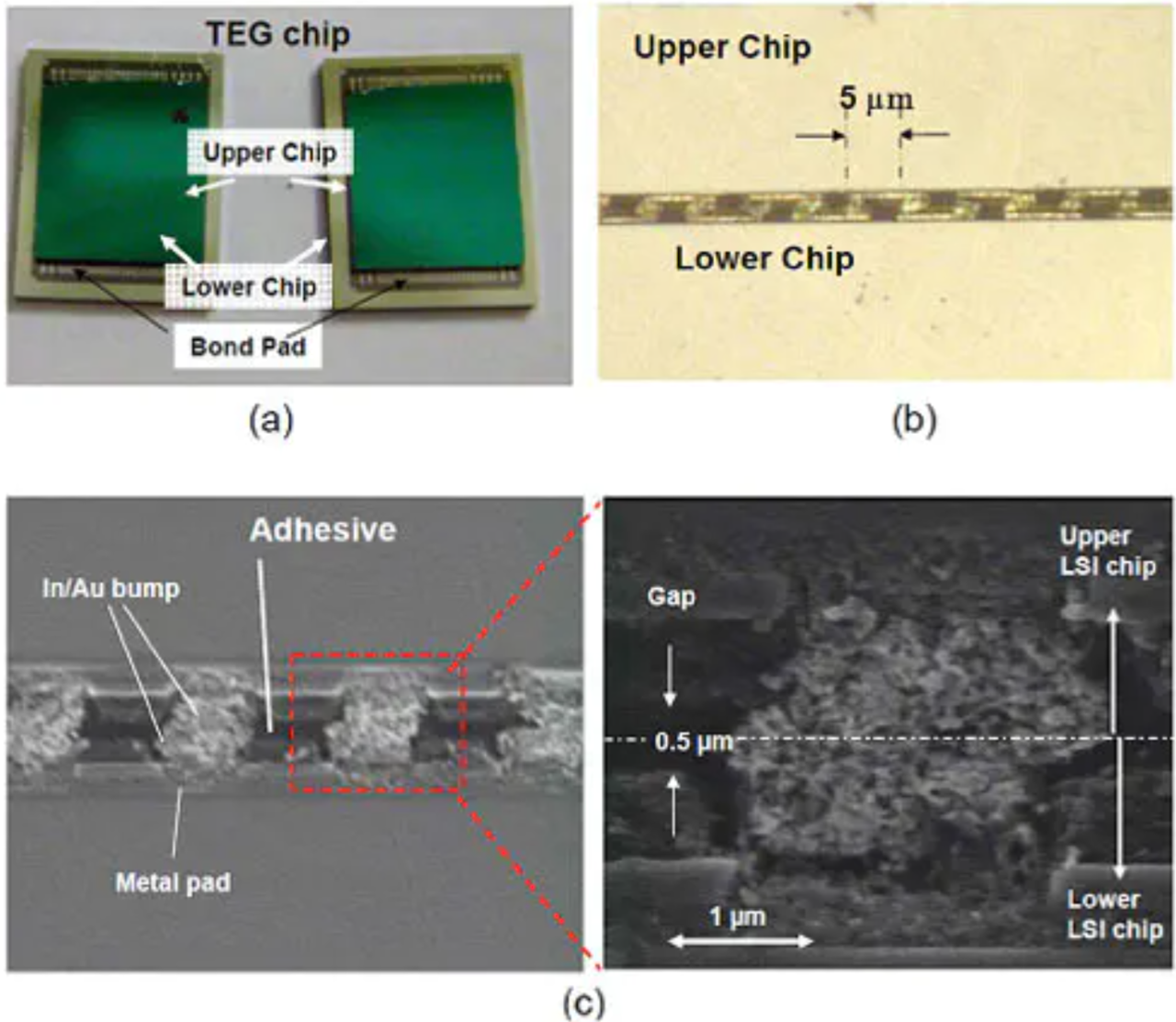
Fig-1:Stacked TEG chip by μ-bumps
The bump size is 2 μm×2 μm. The adhesive is injected after temporary bonding is achieved. The 0.5 μm gap between two chips is completely filled with the adhesive. The bump resistance is less than 0.2 Ω. The results of the temperature cycle test (-65 ℃/150 ℃) revealed that there was no degradation up to 500 cycles. Since the bumps completely melted, the bump resistance did no increase even at a slight misalignment.
Fig-2 is a SEM cross-sectional image of a prototype chip manufactured in T-Micro’s 3D-Stacking LSI prototype manufacturing service by use of our μ-bumps. The bump size is 3 μm×3 μm with 13 μm-pitch.
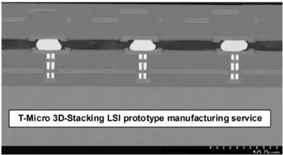
Fig-2:SEM cross-sectional image of a prototype chip
More info: info@t-microtec.com

English Site Menu
Company
Technology
Foundry service
Service case study