TSV・3D-IC製作受託可能
φ12インチまでの専用ライン完備
TEGウエハー製作受託可能
ホーム(日本語ホームページはこちら)
会社概要
活動報告
TMicroの技術
新着情報
三次元LSIとは
サービス・製品
お問い合わせ
HOME
Company
About us
Management
Technology
Technology overview
Fine-pitch Micro-TSV
Micro-Bump
Au cone bump
Au Cylinder Bump
Process facilities
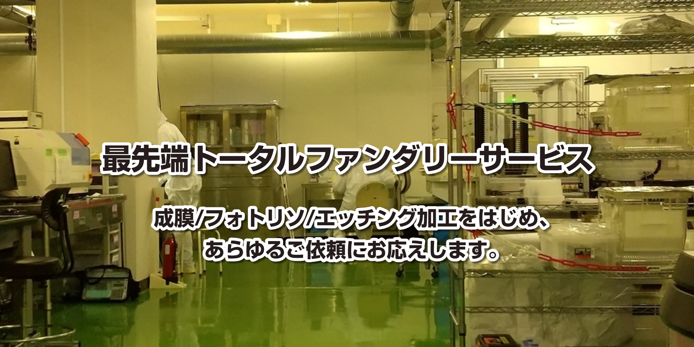
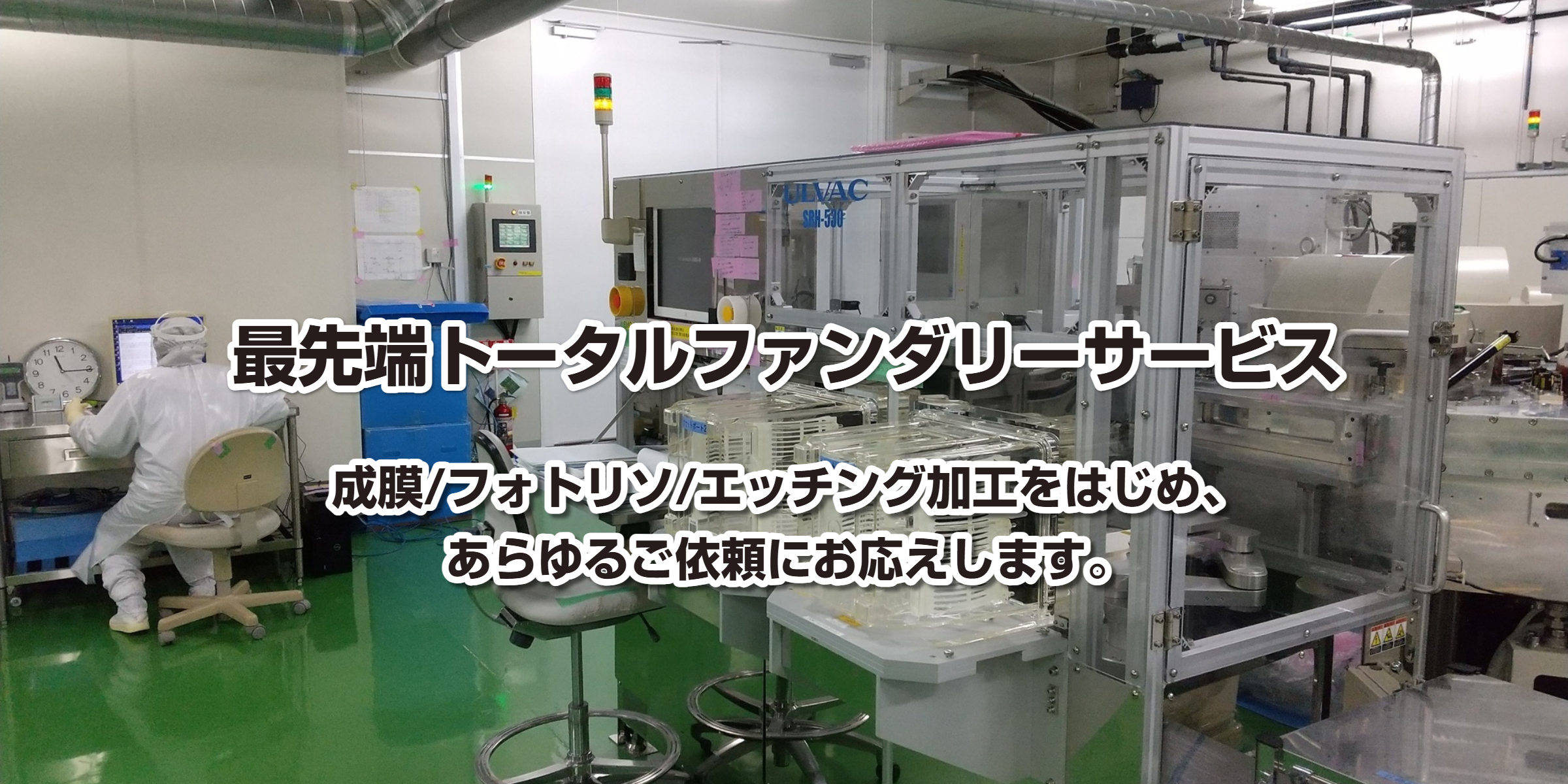
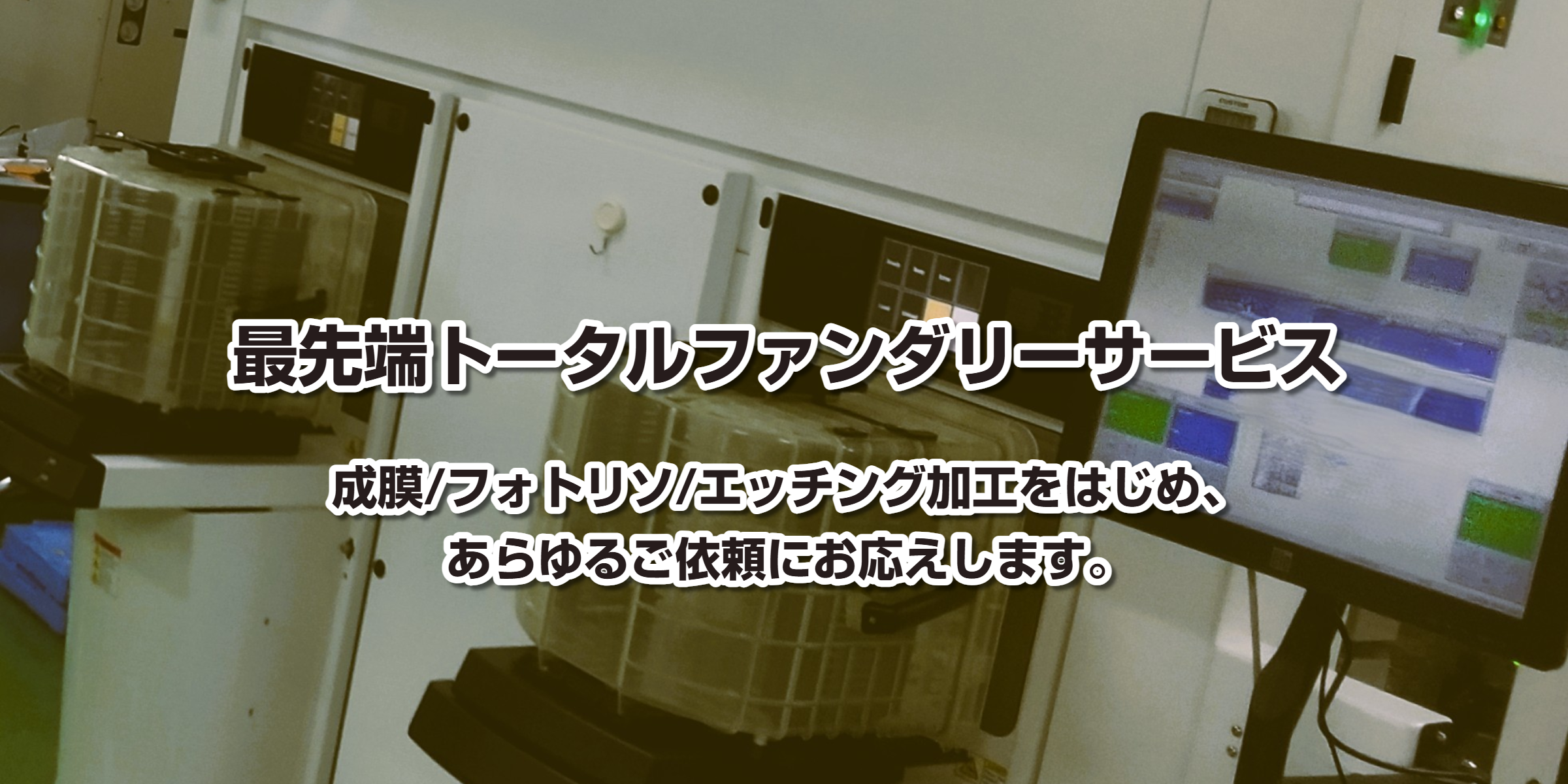
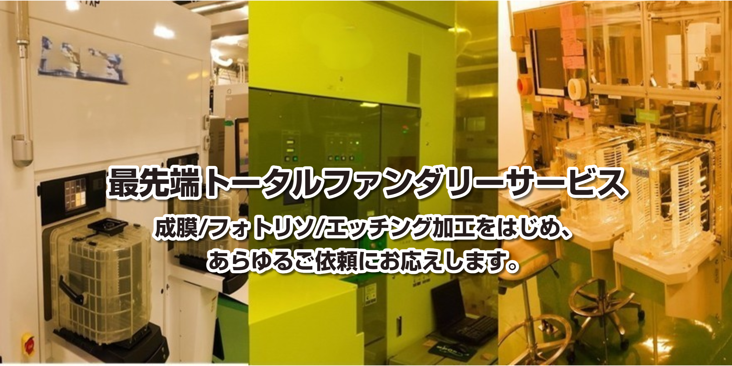
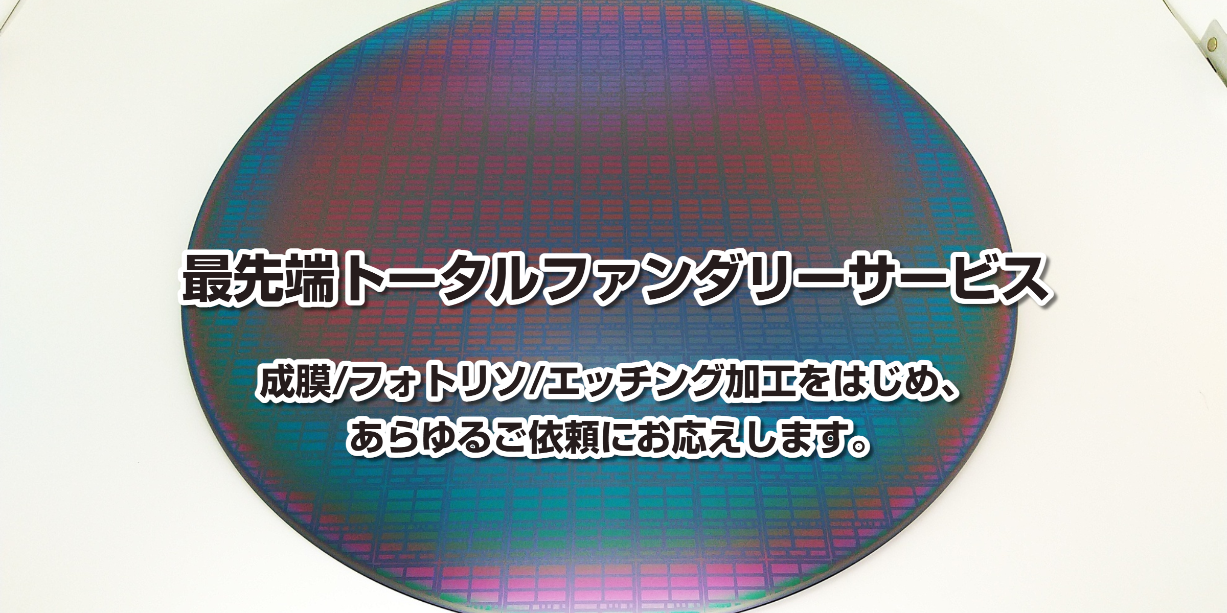
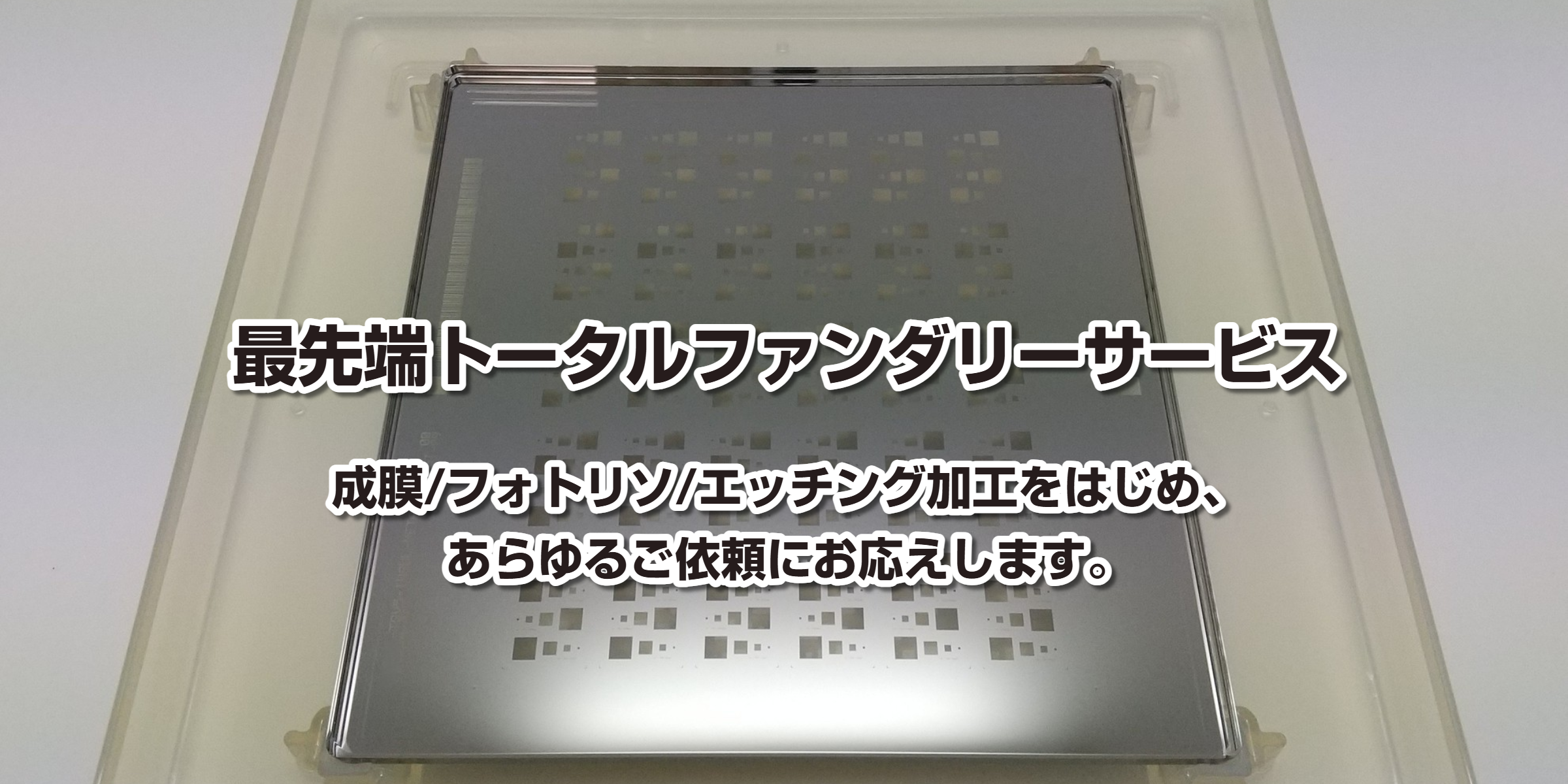
Foundry service
3D-IC process
Si Interposer
Partial process
Service case study
Pixel detector
3D stacking projects
Si Interposer projects
Bilateral Si Microprobe
Optical waveguide Si probe
Download
News & Events
Contact us
〒980-8579 宮城県仙台市青葉区 荒巻字青葉6-6-40 T-Biz203